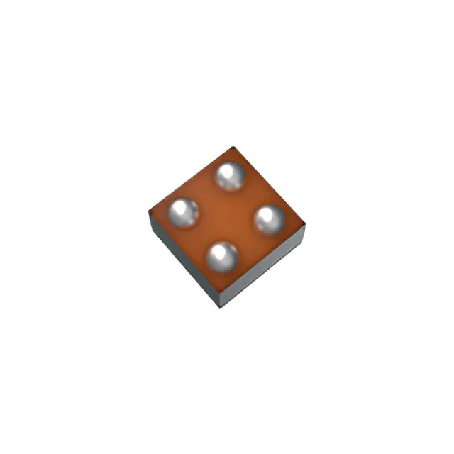
1A high-side load switch in 0.65 mm CSP
The TCK126BG,LF is a single-channel high-side load switch from Toshiba, built around a P-channel MOSFET with a typical on-resistance of 343 mOhm. The switch is controlled by a simple On/Off logic input (non-inverting, 1:1 ratio) and requires no external Vcc supply — the gate drive is derived from the load voltage itself. This makes it a drop-in power-rail gating component for battery-powered or low-standby-power designs.
Slew-rate control and conduction loss
The slew-rate controlled turn-on limits inrush current into capacitive loads, preventing upstream supply droop and reducing EMI. For a 1 µF bypass cap at the switch output, the controlled ramp keeps the peak inrush well below the 1 A current limit, which is useful when sequencing power domains on a PCB.
Housed in a 4-bump WCSPG package measuring 0.65 mm x 0.65 mm (supplier device package 4-WCSPG), the TCK126BG,LF is suited for space-constrained layouts in smartphones, wearables, IoT modules, and other compact PCBs. The 0.4 mm typical bump pitch requires careful PCB land pattern design and solder paste stencil thickness control to avoid bridging. Standard moisture sensitivity level (MSL) precautions apply for the CSP package — verify the MSL rating on the latest Toshiba packing specification before opening the reel.