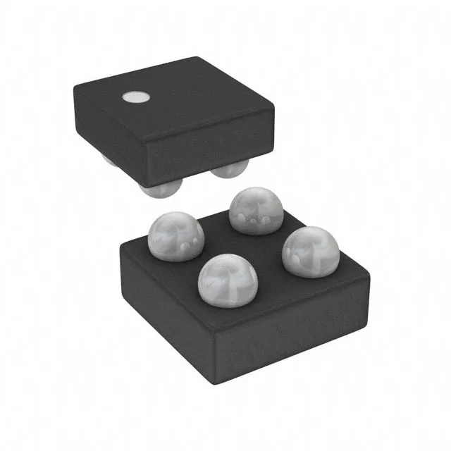
1A high-side switch with 34mOhm typical on-resistance
The Toshiba TCK108AG,LF is a single-channel P-channel high-side load switch rated for 1A continuous output current with a typical Rds(on) of 34mOhm. The 1.1V to 5.5V load voltage range covers common core rails (1.2V, 1.8V, 3.3V) and I/O supplies (5V) in portable and embedded systems. The 34mOhm typical on-resistance at 1A yields a conduction loss of roughly 34mW — negligible in most battery-powered designs, but the actual junction temperature rise depends on the PCB copper area under the 0.79x0.79mm WLCSP package.
Load discharge and slew rate control
Two integrated features manage power-up and power-down behaviour: the slew-rate controlled turn-on limits inrush current into capacitive loads, and the load discharge function pulls the output to ground when the switch is disabled, preventing floating output rails that could hold downstream logic in an indeterminate state. The non-inverting On/Off interface means the switch conducts when the control pin is high — standard active-high logic that simplifies connection to a GPIO from an MCU or SoC without needing an external inverter.
Package and board-fit: 4-bump WLCSP
Housed in a 4-bump wafer-level chip-scale package (WLCSP) measuring 0.79 x 0.79 mm, the TCK108AG,LF requires a PCB land pattern matching the Toshiba recommended footprint — typically a 2x2 array of 0.25mm diameter solder balls on 0.4mm pitch. The tiny footprint suits space-constrained designs like smartphones, wearables, and IoT modules. Surface-mount assembly with Tape & Reel or Cut Tape packaging. The WLCSP package has no exposed thermal pad; heat dissipation relies on the PCB copper plane under the package and the solder balls themselves.