P-channel high-side load switch — 1.54 A, 31 mOhm
The Toshiba TCK1024G,LF is a single-channel P-channel high-side load switch with a 1:1 input-to-output ratio, delivering up to 1.54 A continuous output from a load voltage range of 1.4 V to 5.5 V. Typical on-resistance is 31 mOhm, which keeps conduction losses low in battery-powered and point-of-load distribution — at 1 A the I²R loss is under 31 mW, negligible for most portable designs. Integrated fault protection includes fixed current limiting, over-temperature shutdown, and reverse-current blocking — the reverse-current protection prevents back-feed from the load side when the switch is off, a common requirement in multi-rail power sequencing.
Control interface and load-discharge feature
The switch is controlled by a single non-inverting On/Off logic input — a GPIO from a microcontroller or system controller directly enables the output rail without an external level shifter. A built-in load-discharge feature actively pulls the output to ground when the switch is turned off, preventing floating output rails that could cause erratic behaviour in downstream logic or hold-up in capacitive loads.
Package and board integration — 6-WCSPE
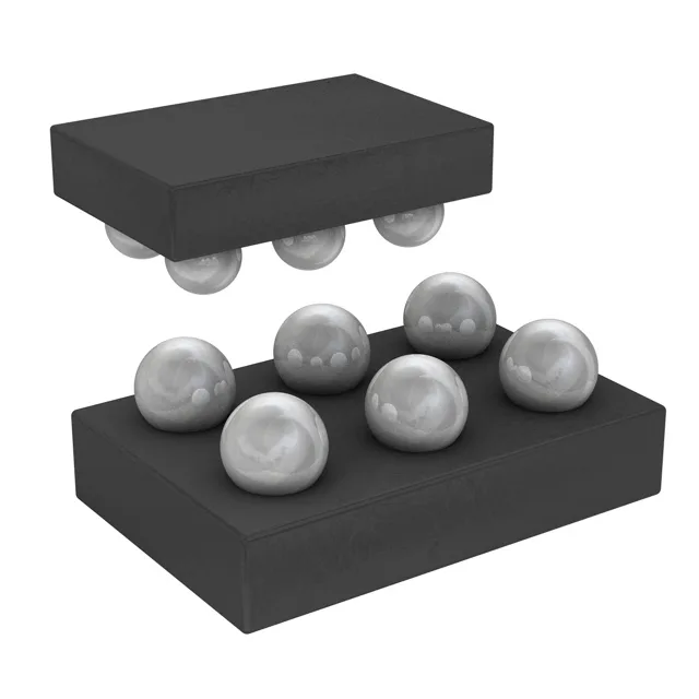
Supplied in a 6-UFBGA, WLCSP package (Toshiba designation WCSPE) with a body size of 0.80 mm x 1.2 mm — the 0.4 mm pitch ball grid array demands a controlled reflow profile and careful solder-paste stencil design to avoid bridging. Surface-mount assembly; the small footprint suits space-constrained PCBs in wearables, IoT modules, and handheld instruments.