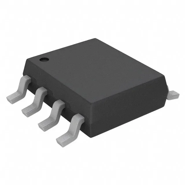
Three inverters in a 2.80 mm-wide package
The TC7WHU04FU,LJ(CT packs three independent inverter gates into an 8-TSSOP or 8-MSOP package measuring just 2.80 mm wide — a compact footprint for signal conditioning on dense boards. Each gate accepts a single input and outputs its logical complement, with Schmitt-trigger hysteresis on the input stage to clean up noisy or slow-rising signals.
7 ns propagation delay at 5V — fast enough for most digital glue
Maximum propagation delay is 7 ns at 5V with a 50 pF load — this sets the data-rate ceiling for the inverter chain; a 7 ns delay means the output settles within one clock period at roughly 70 MHz, though practical toggle rates will be lower due to rise-time effects. Quiescent current is just 2 µA maximum — negligible in battery-powered or always-on circuits where every microamp counts.
Input thresholds span 1.8V to 5V logic
The low-level input threshold is 0.3V and the high-level threshold is 1.7V, making the part compatible with 1.8V logic as well as 3.3V and 5V families — a single inverter can bridge between a 1.8V sensor output and a 3.3V microcontroller input. The supplier device package is listed as 8-SSOP, which shares the same footprint as the 8-TSSOP/MSOP — confirm the specific package variant against your PCB land pattern.
Active production — ROHS3 compliant
ROHS3 compliant, meeting current European lead-free and substance-restriction requirements for electronic assemblies.