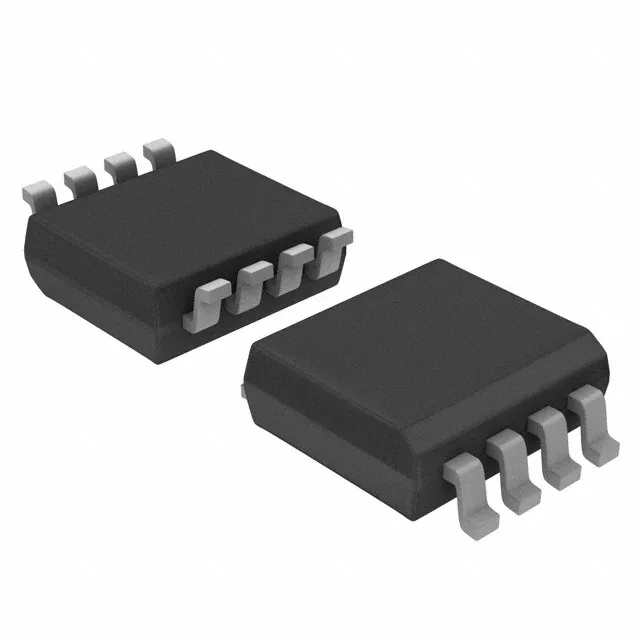
Dual 2-input AND gate in a compact 8-SSOP
The TC7WH08FK,LJ(CT is a dual 2-input AND gate from Toshiba's TC7WH series, a high-speed CMOS logic family. Each of the two independent gates performs the Boolean AND function on its two inputs, making it a basic building block for gating, masking, or enable logic in digital circuits. The wide supply tolerance means a single part can serve in both a 3.3V microcontroller interface and a 5V peripheral bus without a level translator.
Parametric fit: speed, drive, and thresholds
Maximum propagation delay is 7.9ns at 5V with a 50pF load. This 125 MHz equivalent toggle rate at 5V keeps the gate transparent in most SPI, I2C, and parallel bus applications — the delay adds less than one clock cycle at typical bus speeds. Output drive is 8mA source and 8mA sink at the rated supply voltage. That's enough to directly drive a standard LED indicator (with a series resistor) or fan out to up to four LSTTL loads without an external buffer. Input logic thresholds are fixed: low at 0.5V max, high at 1.5V min across the supply range. This 1V hysteresis-like gap provides noise immunity — a 3.3V signal with 300mV of ringing on a long trace still resolves correctly at the gate input. Quiescent current is 2µA maximum. In battery-powered or always-on circuits, the gate's own draw is negligible — a sensor node that sleeps for months loses less charge to the logic than to the leakage of the decoupling capacitor.
The TC7WH08FK,LJ(CT comes in an 8-VFSOP package (0.091" body width, 2.30mm) with a supplier device package designation of 8-SSOP. The 0.65mm pin pitch and 1.25mm body height make it hand-solderable with a fine-tip iron and magnification — a good fit for prototype rework or small-batch assembly. The package is surface-mount only. The narrow 2.30mm width means it fits on a 0.6-inch-wide PCB strip, useful for dense multi-layer boards where real estate is tight.
Lifecycle and compliance
It is ROHS3 compliant (EU 2015/863), with no restricted substances above the threshold limits.