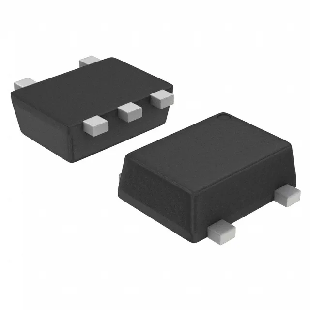
SOT-553 footprint and board integration
The TC7SZ86FE,LJ(CT: The narrow pad geometry demands a controlled solder-paste stencil aperture to avoid bridging between the output and supply pins.
Supply range and timing margin
Operating from 1.65 V to 5.5 V, this gate bridges logic domains without a dedicated level translator — a 1.8 V microcontroller output drives the input, and the 5 V-tolerant output swings to the rail voltage. Quiescent current maxes at 2 µA — negligible in a battery-powered sensor node that spends most of its time in a low-power sleep state with the gate inputs held at a valid logic level.
Output drive and fan-out
Each output sources or sinks 32 mA, enough to drive three to five standard LSTTL loads or a single LED through a current-limiting resistor without a buffer. The 32 mA symmetric drive also means the rise and fall times stay matched within 1 ns at 50 pF, reducing duty-cycle distortion in clock distribution paths.
Lifecycle and compliance posture
ROHS3 compliant, so it clears EU and UKCA material restrictions without exemption paperwork. The TC7SZ series is a mature logic family; second-source equivalents from other vendors (same functional XOR in SOT-553) exist but require pin-to-pin validation of the input threshold levels at the low end of the supply range.