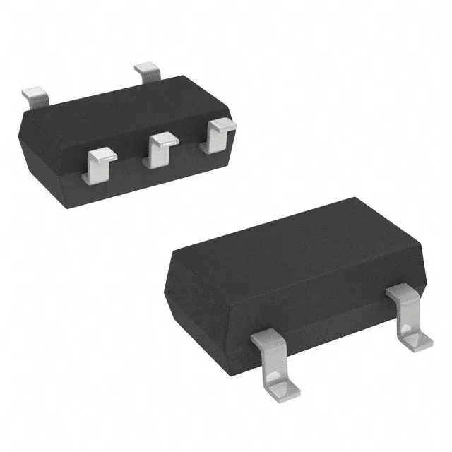
Toshiba Semiconductor RN2701,LF — Discrete Semiconductors

Toshiba RN2701,LF dual PNP pre-biased transistor, 200mW

MPNRN2701,LF
End of Life

Toshiba Semiconductor RN2701 series dual PNP pre-biased transistor (BRT), 5-TSSOP/SC-70-5/SOT-353 package, 200mW, 50V Vce, 100mA Ic, 200MHz Ft, 4.7kohm base & emitter resistors.

$0.29Ref. price · indicative, final on quote
Packaging5-TSSOP, SC-70-5, SOT-353
StockContact for availability
Lead timeIn Stock wk
MOQ1 pcs
  • 100% new & originalTraceable channels only — no refurbs, no pulls, no remarked parts.
  • Date & lot codes on quoteStated per line before you commit; label photos on request.
  • MSL-compliant ESD packingMoisture-sealed bags with indicator cards; reels photo-verified.
  • PayPal buyer protectionPay by T/T, PayPal or Payoneer — card payments covered end to end.

Specifications

RN2701,LF Technical Specifications
ParameterValue
Mounting typeSurface Mount
FET type2 PNP - Pre-Biased (Dual)
Voltage - collector emitter breakdown50V
Current - collector (Ic)100mA
Current - collector cutoff500nA
DC current gain (hFE) (Min) @ ic, vce30 @ 10mA, 5V
Power - max200mW
Frequency200MHz
PackageTape & Reel (TR); Cut Tape (CT)
Case5-TSSOP, SC-70-5, SOT-353
Resistor - base (R1)4.7kOhms
Resistor - emitter base (R2)4.7kOhms
Vce saturation (Max) @ ib, ic300mV @ 250µA, 5mA

Product details

SOT-353 dual PNP with integrated bias resistors

The RN2701,LF packs two PNP transistors with monolithic base (R1) and emitter-base (R2) resistors, each 4.7 kΩ, into a 5-pin SOT-353 (SC-70-5) package — the bias network is on-die, so the BOM loses two resistor placements and the associated pick-and-place cost. Surface-mount, tape-and-reel or cut-tape delivery. The USV supplier device package code is Toshiba's internal mark for the SOT-353 outline — the footprint matches the industry-standard SC-70-5 land pattern.

200 mW power ceiling and 50 V breakdown

Each transistor is rated for 50 V collector-emitter breakdown and 100 mA continuous collector current, with a total package dissipation of 200 mW — the limiting factor in a dense board is the copper area under the SOT-353, not the silicon itself. Transition frequency is 200 MHz, so the part handles low-frequency switching and digital-level translation comfortably; the 300 mV Vce saturation at 250 µA base / 5 mA collector means the output drop stays under a logic-low threshold when driving a CMOS input. Minimum DC current gain is 30 at 10 mA collector current, 5 V Vce — the pre-biased resistors set the base current, so the actual gain in circuit is fixed by the resistor ratio, not external components.

Frequently asked questions

What is the closest functional second-source for RN2701,LF?

The RN2701JE(TE85L,F) shares the same 4.7 kΩ base and emitter resistors, 200 MHz Ft, and 50 V / 100 mA ratings, but its package dissipation is 100 mW (half the 200 mW of RN2701,LF) and the transistor pair is emitter-coupled rather than independent — the board layout and thermal budget differ.

Will RN2701,LF drop into a board laid out for RN2701JE(TE85L,F)?

Both parts are in SOT-353 (SC-70-5) with the same pinout for dual PNP BRTs — the land pattern is identical. The functional difference is the emitter coupling on the JE variant and the lower 100 mW power limit; the RN2701,LF is a drop-in with higher dissipation headroom.

What compliance documentation does Toshiba provide for RN2701,LF?

The part is ROHS3 compliant. Toshiba supplies a material declaration and REACH/SVHC statement per standard semiconductor industry practice — no UL or IEC certification is listed for this discrete transistor.