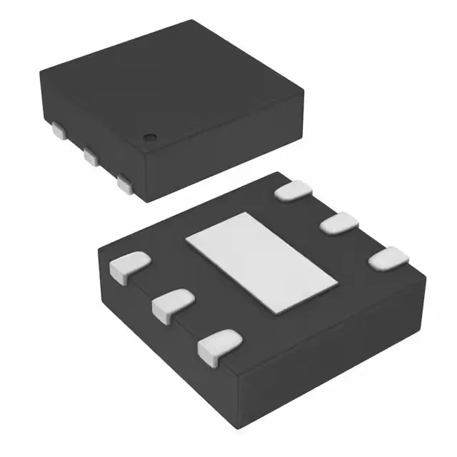
Texas Instruments UCC27512MDRSTEP — Power Management (PMIC / Gate Driver)

UCC27512MDRSTEP Low-Side Gate Driver, 4A/8A Peak, 6-SON

MPNUCC27512MDRSTEP
Active

Texas Instruments UCC27512MDRSTEP, low-side gate driver, single channel, 4A source / 8A sink peak output, 8ns rise / 7ns fall, 4.5V to 18V supply, -55°C to 125°C, 6-WDFN Exposed Pad (6-SON 3x3), Tape & Reel.

$4.4700Ref. price · indicative, final on quote
Packaging6-WDFN Exposed Pad
RoHSROHS3 Compliant
Independent supplier — new & surplus stockAuthenticity-screened · ESD-safe packingListing updated Aug 2026

Specifications

UCC27512MDRSTEP specifications
ParameterValue
Gate typeIGBT, N-Channel MOSFET
Input typeInverting, Non-Inverting
Channel typeSingle
MountingSurface Mount
Supply voltage4.5V ~ 18V
Logic voltage - VIL, VIH1V, 2.4V
Current - peak output (Source, sink)4A, 8A
Operating temperature-55°C~125°C(TJ)
PackageTape & Reel (TR); Cut Tape (CT)
Case6-WDFN Exposed Pad
Number of drivers1
Driven configurationLow-Side
Rise (Fall time)8ns, 7ns

Product details

Single-channel low-side driver with 4 A / 8 A peak drive

The driver operates from a 4.5 V to 18 V supply rail and is specified over a junction temperature range of -55°C to 125°C, suiting it for military, aerospace, and industrial environments where wide thermal margins are required.

Input logic thresholds and configuration flexibility

The UCC27512 accepts both inverting and non-inverting input signals, with logic thresholds set at 1 V (VIL) and 2.4 V (VIH).

Housed in a 6-SON (3 mm x 3 mm) package with exposed pad, the device relies on the pad for heat sinking.

It is ROHS3 compliant, meeting current environmental requirements for global shipping.

Frequently asked questions

Can UCC27512MDRSTEP drive two MOSFETs in parallel?

Yes, the 4 A source / 8 A sink peak output current provides enough drive strength to switch two paralleled MOSFETs with moderate gate charge, provided the total gate charge does not exceed the driver's peak current capability at the desired switching frequency. The 8 ns rise / 7 ns fall times help maintain fast switching edges even with increased capacitive load.

What is the recommended PCB layout for UCC27512MDRSTEP?

The exposed pad (6-SON, 3x3 mm) must be soldered to a thermal land on the PCB with via stitching to an internal ground plane for heat dissipation. Place a 1 µF to 10 µF ceramic decoupling capacitor as close as possible to the VDD and GND pins. Keep the gate-drive loop short to minimize parasitic inductance.

Is UCC27512MDRSTEP RoHS compliant?

Yes, it is ROHS3 Compliant per the listing.