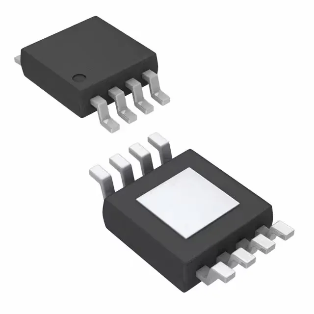
Dual 4A low-side driver for N- and P-channel gates
It drives both N-channel and P-channel MOSFETs, making it a single-part solution for synchronous rectifier stages, half-bridge topologies, and secondary-side post-regulation in isolated supplies. Each channel operates independently with non-inverting input logic, and the logic thresholds are set at 1V (VIL) and 2V (VIH), which means 3.3V logic interfaces directly without level translation.
The 20ns rise and 15ns fall times (typical) at 4A peak output mean the driver can charge and discharge the MOSFET gate capacitance quickly, reducing cross-conduction dead-time margin in a synchronous buck. For a 10 nC gate charge, the effective switching time is under 5 ns per amp — fast enough for 500 kHz to 1 MHz switching frequencies without excessive Miller plateau dwell. The 4V to 15V supply range covers both 5V and 12V bias rails common in industrial power supplies and telecom bricks. At 4V the driver still delivers full 4A peak current, though the on-resistance of the output stage rises slightly — the datasheet's typical curves show the output voltage swing stays within 0.5V of the rail at 4A.
Package and temperature grade — board-level fit
The exposed pad is electrically connected to the substrate (GND), so the PCB thermal via pattern must connect to the ground plane. Store the reels in a dry cabinet below 10% RH if the moisture-barrier bag is opened; the MSL level is not listed here, but the exposed-pad HVSSOP typically rates MSL-3 (168-hour floor life).