9 A peak drive — what it buys you
The UCC27322PE4 delivers 9 A peak source and 9 A peak sink current, enough to charge and discharge the gate capacitance of large N-channel and P-channel MOSFETs in a few tens of nanoseconds. That 20 ns typical rise and fall time keeps switching losses low even at moderate frequencies, which matters when you are driving a parallel bank of FETs or a single big IGBT module.
Low-side only — where it fits
This is a single-channel, non-inverting low-side driver. The driven configuration is low-side, meaning the MOSFET source connects to ground and the gate driver pulls the gate above source to turn it on. It will not drive a high-side FET directly — for that you need a bootstrap or isolated supply.
4 V to 15 V supply — compatibility check
The supply range spans 4 V to 15 V, covering standard 5 V and 12 V gate-drive rails. At the low end, 4 V is marginal for driving standard-threshold MOSFETs to full Rds(on) — you will want logic-level FETs if you run the supply near 4 V. At 12 V the driver has headroom for most standard-threshold power MOSFETs and IGBTs.
Through-hole package — rework and reliability
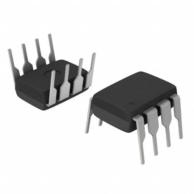
The 8-pin DIP (0.300-inch body, 7.62 mm row spacing) in PDIP plastic is a through-hole package. That means it survives multiple soldering cycles, is easy to hand-replace with a desoldering tool, and stands up to vibration better than an SOIC in a socket. No MSL concerns — PDIP is moisture-insensitive.
That means TI has announced end-of-life and will accept final orders within a defined window. Once that window closes, the part will no longer be manufactured. If you have an active design using this exact order code, now is the time to secure lifetime-buy quantities or qualify a pin-compatible replacement.