That combination means it can charge a 10 nC gate capacitance in roughly 2.2 ns at the Miller plateau, which keeps the switching transition short and the crossover conduction loss low in hard-switched topologies.
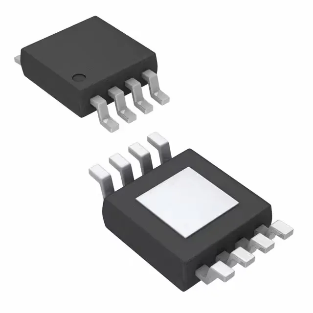
Package and thermal: the exposed pad is part of the circuit
The single driver channel occupies one output pin; the adjacent pins carry the supply and ground returns. The layout should keep the gate-drive loop (driver output → gate resistor → MOSFET gate → source → ground return) under 1 cm to minimise parasitic inductance that would otherwise slow the edge or cause ringing.