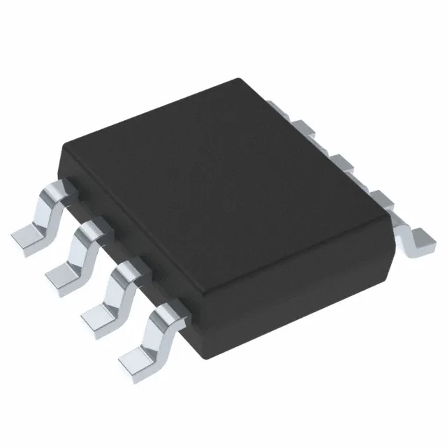
Texas Instruments UCC27201ADDA — Power Management (PMIC / Gate Driver)

UCC27201ADDA 3A Half-Bridge MOSFET Driver, 8ns/7ns

MPNUCC27201ADDA
Active

Texas Instruments UCC27201ADDA, half-bridge N-channel MOSFET driver, 3A peak source/sink, 8ns rise / 7ns fall, 8 V to 17 V supply, 120 V bootstrap max, -40°C to 140°C junction, 8-PowerSOIC (0.154", 3.90 mm width) surface mount.

$3.3000Ref. price · indicative, final on quote
Independent supplier — new & surplus stockAuthenticity-screened · ESD-safe packingListing updated Jul 2026

Specifications

UCC27201ADDA specifications
ParameterValue
Gate typeN-Channel MOSFET
Input typeNon-Inverting
Channel typeIndependent
MountingSurface Mount
Supply voltage8V ~ 17V
Logic voltage - VIL, VIH0.8V, 2.5V
High side voltage - max (Bootstrap)120 V
Current - peak output (Source, sink)3A, 3A
Operating temperature-40°C~140°C(TJ)
PackageBulk
Case8-PowerSOIC (0.154\", 3.90mm Width)
Number of drivers2
Driven configurationHalf-Bridge
Rise (Fall time)8ns, 7ns

Product details

The 8 ns typical rise time and 7 ns fall time at 1 nF load keep switching losses low enough that the designer can push the switching frequency into the hundreds of kilohertz without the driver becoming the thermal bottleneck. The bootstrap supply supports a high-side rail up to 120 V, which covers 48 V bus converters, 72 V telecom bricks, and 100 V intermediate bus architectures with margin.

Supply rails and logic thresholds — fitting the bias architecture

The driver operates from a single 8 V to 17 V bias rail, which matches the standard 12 V or 15 V auxiliary supply found in most power converters. The logic input thresholds are 0.8 V (VIL) and 2.5 V (VIH), so a 3.3 V PWM controller output drives the inputs directly without a level-shifter. The non-inverting input type means the output follows the input polarity — no inversion to account for in the control loop.

Thermal and package — the PowerPad matters for the current loop

The surface-mount footprint is the same 3.90 mm width as a standard SOIC-8, but the pad pattern differs; the PCB layout must include the exposed-paddle land.

The SO PowerPad package is a standard TI footprint, and the part shares the same die and pinout as the rest of the UCC27201 family, differing only in the package variant.

Frequently asked questions

What is the price of UCC27201ADDA?

Buyers need to compare costs across distributors and determine budget fit.

Is UCC27201ADDA in stock?

Availability directly impacts procurement timeline and production schedules.

What is the pinout of UCC27201ADDA?

Design engineers must validate PCB layout and compatibility with existing circuit.

What are the alternatives for UCC27201ADDA?

Buyers explore substitutes to mitigate supply risk or find better pricing.

What is the operating voltage range for UCC27201ADDA?

Ensures the driver is compatible with the system’s power supply voltage level.

Is UCC27201ADDA still in production?

Brokers and engineers need lifecycle status to avoid obsolete parts in designs.