55 dB PSRR at 1 kHz — the analog supply rail decision
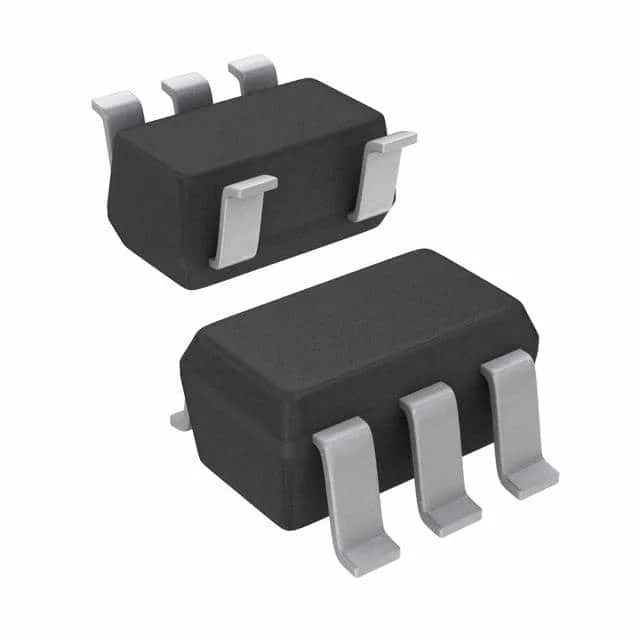
The TPS7A0312PDBVR is a 200 mA LDO from Texas Instruments with a fixed 1.2 V output, housed in a SOT-23-5 package. Its 55 dB power-supply rejection ratio at 1 kHz attenuates switching ripple from a preceding buck converter by a factor of about 560 — enough to keep a 10 mVpp switching artifact below 20 µVpp at the output, which matters when this rail feeds an analog front-end or a precision ADC reference. The 300 nA quiescent current is the defining spec for always-on, battery-powered applications. The LDO's own draw sits below the self-discharge rate of a small lithium coin cell, so a sensor node that spends most of its life in sleep mode loses more capacity to the battery's internal chemistry than to the regulator.
Dropout headroom and thermal envelope
Maximum dropout voltage is 0.7 V at the full 200 mA load. The enable pin (active high) allows the system to gate the output when the load is idle, cutting the quiescent current to near zero. Operating junction temperature range is -40°C to 125°C, placing this part in the industrial/automotive temperature band. An engine-bay ECU or an outdoor IoT node that sees 105°C ambient still has 20°C of junction margin at full load, assuming a typical 50°C/W θJA for the SOT-23-5 on a standard two-layer board.
Protection features and package integration
Built-in protection includes over-current, over-temperature, and under-voltage lockout (UVLO). The UVLO threshold prevents the output from turning on until the input rail is high enough to keep the pass element in saturation, avoiding a brown-out condition on the load. The SOT-23-5 footprint (SC-74A) has a 0.95 mm pin pitch — the enable pin sits on pin 3, so the layout must route the enable trace away from the output capacitor's ground return to avoid coupling noise into the feedback path.