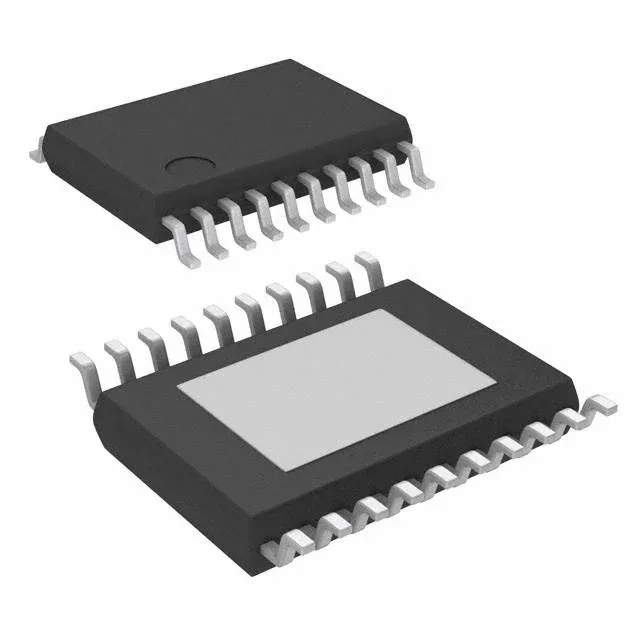
20-HTSSOP footprint and thermal management
The TPS60130PWPR: The 0.65mm pin pitch and 4.4mm body width mean a standard 20-pin TSSOP footprint works, but the centre pad opening in the solder paste stencil should be segmented to avoid voiding. Tape & Reel (TR) is the production format; Cut Tape (CT) is available for bench builds.
Step-up charge pump — inductor-free 5V rail
This is a charge-pump topology, not a switched-inductor boost. The 320kHz switching frequency drives two external flying capacitors to double or triple the input voltage to a fixed 5V output. The absence of an inductor means the radiated EMI profile is cleaner than a boost converter, but the 300mA output ceiling is lower than what an inductor-based part would deliver from the same 2.7-5.4V input range. No synchronous rectifier is integrated — an external Schottky diode is required in the charge-pump stage. The diode's forward drop reduces efficiency at low input voltage, but the part avoids the shoot-through risk and BOM cost of an integrated synchronous FET.
Lifecycle and compliance posture
ROHS3 compliant, no exemption conflicts for EU or global markets. Sourced through authorised and independent distribution channels.
What the ratings mean for the BOM line
The fixed 5V output at 300mA covers small logic rails, sensor supplies, and MCU I/O banks. The 2.7V minimum input means it can run from a 3-cell NiMH stack or a single Li-ion cell through most of its discharge curve. The 5.4V maximum input limits it to regulated 5V rails or lower — do not connect it to an unregulated 12V bus. For under-hood or chassis-mounted applications, verify the TI qualification status separately.