1.1 A high-side switch with 100 mOhm Rds(on)
The TPS2551DRVTG4 is a single-channel, high-side power distribution switch from Texas Instruments, designed for general-purpose load switching in 2.5 V to 6.5 V systems. It integrates an N-channel MOSFET with a typical on-resistance of 100 mOhm, delivering up to 1.1 A continuous output. The switch is controlled by an On/Off interface with non-inverting input logic, and the output ramps at a controlled slew rate to limit inrush current. The 1.1 A current rating and 100 mOhm Rds(on) define the conduction loss floor: at full load the voltage drop is roughly 110 mV, and the I²R dissipation is about 121 mW.
Fault protection: adjustable current limit, thermal shutdown, UVLO
The TPS2551 integrates three protection mechanisms. The current limit is adjustable via an external resistor, letting the designer set the threshold between the 1.1 A maximum and a lower limit matched to the load and wiring. Over-temperature shutdown protects the switch and downstream circuitry if the die exceeds the safe junction temperature. Undervoltage lockout (UVLO) holds the output off when the supply rail drops below the operating range, preventing the MOSFET from operating in the linear region. For a battery-powered or USB port application, the adjustable current limit is the key feature — it lets the designer set the trip point just above the load's normal peak draw, so a short or overload trips the switch before the PCB trace or connector exceeds its current rating.
Package and thermal: 6-WSON with exposed pad
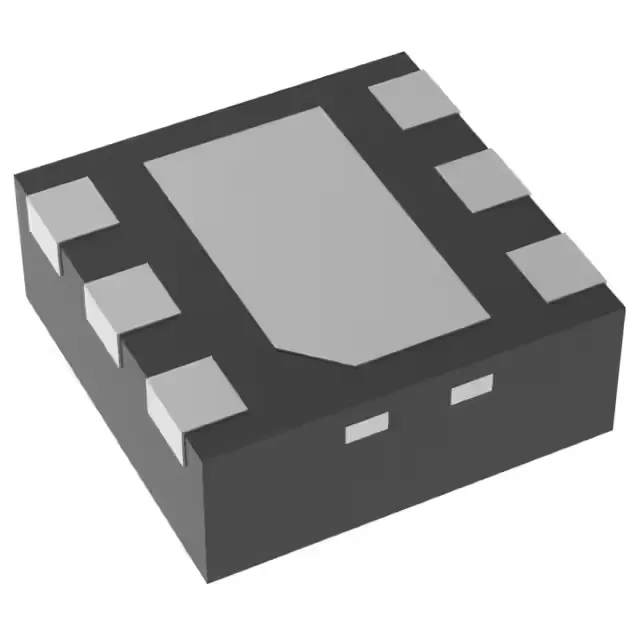
The TPS2551DRVTG4 is supplied in a 6-WDFN exposed-pad package, also designated as 6-WSON (2x2 mm). The small 2x2 mm footprint suits dense layouts, but the thermal resistance depends on the board design — a minimal copper land raises the junction temperature for a given load current. The part is shipped in Tape & Reel (TR) format, standard for automated pick-and-place assembly. The surface-mount package requires no through-hole soldering step.