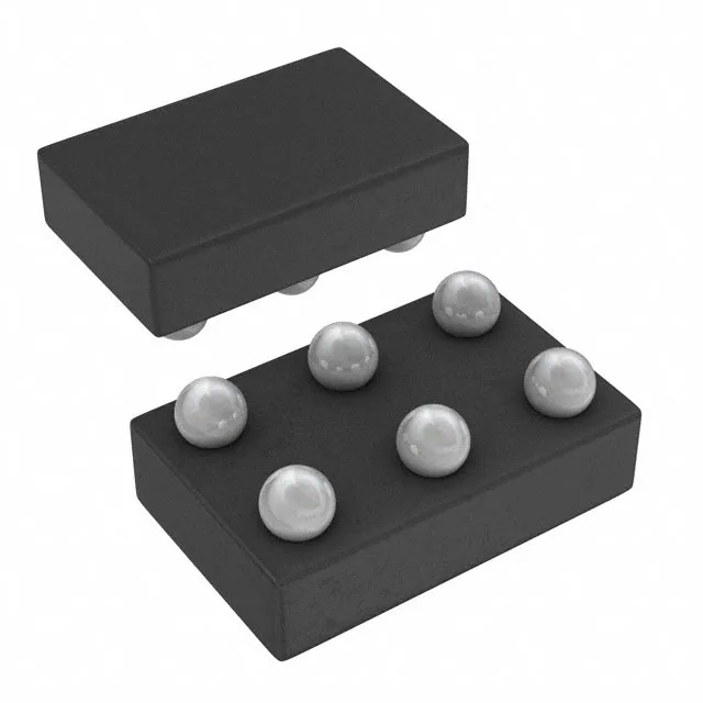
Texas Instruments TPS22924CYZPT — Power Management (PMIC / Gate Driver)

TPS22924CYZPT Texas Instruments Load Switch – 18.3 mOhm, 2 A

MPNTPS22924CYZPT
Active

Texas Instruments TPS22924CYZPT, a general-purpose high-side load switch in a 6-DSBGA package, featuring 18.3 mOhm typical on-resistance, 2 A continuous output, and a 0.75 V to 3.6 V load voltage range.

$1.1300Ref. price · indicative, final on quote
Packaging6-XFBGA, DSBGA
RoHSROHS3 Compliant
Independent supplier — new & surplus stockAuthenticity-screened · ESD-safe packingListing updated Aug 2026

Specifications

TPS22924CYZPT specifications
ParameterValue
Input typeNon-Inverting
Output typeN-Channel
TypeGeneral Purpose
MountingSurface Mount
Voltage - load0.75V ~ 3.6V
Voltage - supply (Vcc (Vdd))Not Required
Output current2A
I/O channels1
InterfaceOn/Off
Operating temperature-40°C~85°C(TA)
PackageTape & Reel (TR); Cut Tape (CT)
FeaturesLoad Discharge, Slew Rate Controlled
Rds on18.3mOhm
Case6-XFBGA, DSBGA
Output configurationHigh Side
Ratio - Input:Output1:1

Product details

What this load switch does on your board

The TPS22924CYZPT is a single-channel, high-side N-channel MOSFET load switch from Texas Instruments. With a typical Rds(on) of 18.3 mOhm, the voltage drop at 2 A is under 40 mV — negligible for most 1.8 V and 3.3 V rails. The slew-rate controlled turn-on limits inrush current, and the integrated load discharge resistor pulls the output to ground when disabled. The 6-DSBGA package (1.39 mm x 0.89 mm) is a wafer-level chip-scale package — no exposed pad, no thermal vias needed for most loads.

Key ratings that matter for your BOM

The 2 A continuous current rating is the absolute maximum at 85°C ambient — derate if the board runs hot or the load is pulsed. The 18.3 mOhm Rds(on) is typical at 3.6 V input; expect it to rise ~25% at 1.8 V and another 20% at 85°C junction. No external Vcc supply is needed — the switch is self-powered from the load voltage pin. This simplifies routing but means the input voltage must be present and stable before the enable pin goes high.

ROHS3 compliant. Sourced per RFQ — confirm lead time and pricing against your BOM quantity.

Design-in checklist for the 6-DSBGA package

The 6-DSBGA package has a 1.39 mm x 0.89 mm body with 6 balls on a 0.5 mm pitch. The recommended land pattern is a 0.25 mm diameter NSMD pad with a 0.3 mm solder mask opening. No thermal pad — the die dissipates through the balls and the PCB copper. The part is rated for industrial environments — outdoor telecom cabinets, factory floor controllers, and automotive cabin modules (non-AEC-Q100).

Frequently asked questions

What is the closest pin-compatible alternative to the TPS22924CYZPT?

Within the same TPS22924 family, the TPS22924CYZPR shares the same 6-DSBGA package and pinout but is offered in a different reel quantity. For a higher-current sibling, consider the TPS22925 series (3 A) in the same package — verify pin compatibility against the datasheet.

What is the Rds(on) and input voltage range of the TPS22924CYZPT?

Typical Rds(on) is 18.3 mOhm. The load voltage range is 0.75 V to 3.6 V. No separate Vcc supply is required.