Load-switch parametrics and the fit decision
The TPS22924BYZT: The integrated slew-rate control limits inrush current during turn-on, and the load-discharge feature pulls the output to ground when the switch is disabled — both are useful when sequencing rails for an SoC or FPGA that cannot tolerate slow discharge or voltage hold-up on a disabled rail.
Package, temperature grade, and board integration
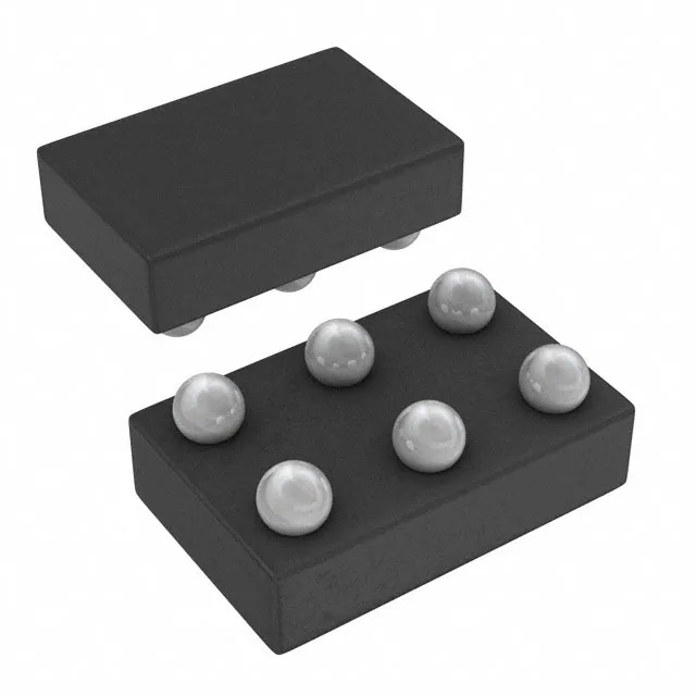
Housed in a 6-bump DSBGA (6-XFBGA) measuring roughly 1.3 mm × 0.9 mm, the TPS22924BYZT demands a fine-pitch PCB layout with via-in-pad or micro-via fan-out for the output and input connections. No external Vcc supply is needed — the switch is self-biased from the input voltage, so the BOM count stays at the switch plus two bypass capacitors.