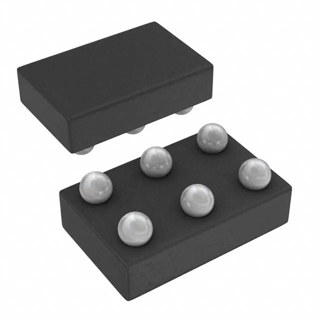
The TPS22924BYZPRB is a single-channel, high-side load switch from Texas Instruments, built around an N-channel MOSFET with a typical Rds(on) of 18.3 mOhm. At 2 A continuous output, that translates to roughly 73 mW of conduction loss at 25°C — negligible for most PCB thermal budgets, but the junction-to-ambient thermal resistance of the 6-DSBGA package means the copper pad area on the board sets the real derating curve. The switch operates from a 0.75 V to 3.6 V load voltage range, covering the core rails of modern SoCs, FPGAs, and PMICs without requiring a separate bias supply (Vcc/Vdd not required).
Load discharge and slew rate control — sequencing without surprises
Two integrated features address common power-sequencing headaches. The load discharge circuit pulls the output to ground when the switch is turned off, preventing a floating output that could hold a downstream regulator in an undefined state. The slew rate controlled turn-on limits inrush current into capacitive loads — useful when the switch feeds a bank of decoupling caps on a processor core rail.
DSBGA-6 footprint — board area vs. assembly trade-off
The 6-DSBGA package measures 1.39 x 0.89 mm — roughly the area of a 0402 resistor.