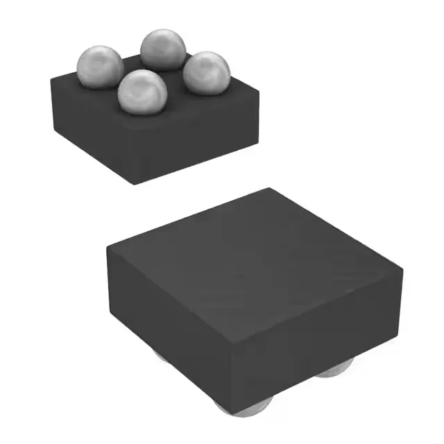
Single-channel high-side load switch in a 4-bump DSBGA
It integrates slew-rate control for controlled inrush current and reverse current protection to block back-feed from the output to the input.
200 mOhm Rds(on) and 2 A load — thermal and drop budget
The typical on-resistance of 200 mOhm at 2 A yields a 400 mV drop and 0.8 W dissipation — within the DSBGA package's capability at 85°C ambient, but the board copper area under the bump array sets the actual thermal resistance. For a 1.8 V rail, that 400 mV drop consumes over 20% of the supply headroom; designs sensitive to voltage loss should budget for the drop or consider a lower-Rds(on) part in a larger package. The 1:1 input-to-output ratio and non-inverting control simplify the enable logic — a logic-high on the ON pin turns the switch on, with no external level-shifting needed for 1.8 V or 3.3 V logic.
4-bump DSBGA — footprint and assembly constraints
The total footprint is approximately 0.8 mm × 0.8 mm, making it suitable for ultra-compact wearables, IoT modules, and portable devices. The package is not hand-solderable — it requires a solder-paste stencil, reflow oven, and X-ray inspection for bump-joint verification.
Industrial temperature grade and fault protection
The reverse current protection blocks current flow from output to input when VOUT exceeds VIN — useful when the load side has a large output capacitor or an independent supply that could back-drive the input rail.