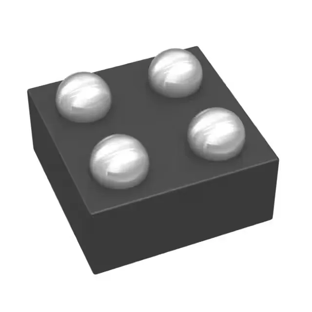
Texas Instruments TPS22914BYFPR — Power Management (PMIC / Gate Driver)

TPS22914BYFPR – Texas Instruments 2 A Load Switch, 4-DSBGA

MPNTPS22914BYFPR
Active

Texas Instruments TPS22914BYFPR, a single-channel N-channel high-side load switch in a 4-bump DSBGA package, rated 2 A continuous output with 37 mOhm typical on-resistance over a 1.05 V to 5.5 V load range.

$0.6000Ref. price · indicative, final on quote
Packaging4-XFBGA, DSBGA
RoHSROHS3 Compliant
Independent supplier — new & surplus stockAuthenticity-screened · ESD-safe packingListing updated Aug 2026

Specifications

TPS22914BYFPR specifications
ParameterValue
Input typeNon-Inverting
Output typeN-Channel
TypeGeneral Purpose
MountingSurface Mount
Voltage - load1.05V ~ 5.5V
Voltage - supply (Vcc (Vdd))Not Required
Output current2A
I/O channels1
InterfaceOn/Off
Operating temperature-40°C~85°C(TA)
PackageTape & Reel (TR); Cut Tape (CT)
FeaturesSlew Rate Controlled
Rds on37mOhm
Case4-XFBGA, DSBGA
Output configurationHigh Side
Ratio - Input:Output1:1

Product details

Active production — what this means for your BOM

2 A output, 37 mOhm — sizing the load switch

Rated for 2 A continuous output current, the TPS22914BYFPR can power a modest peripheral rail, sensor cluster, or sub-regulator input. The 37 mOhm typical Rds(on) at 5 V bias means a voltage drop of roughly 74 mV at full load — negligible for most 3.3 V or 5 V rails, but worth checking against the downstream supply tolerance. The load voltage range spans 1.05 V to 5.5 V, covering common logic and I/O voltages. No external Vcc supply is required — the switch is self-biased from the load voltage.

Slew-rate control and thermal design

The slew-rate controlled turn-on limits inrush current when switching into a capacitive load, which prevents upstream supply droop and reduces EMI. This is a practical feature for power-sequencing or hot-swap applications where a sudden current surge could reset a shared rail.

Package and footprint — what to expect

Housed in a 4-bump DSBGA package, the TPS22914BYFPR requires a fine-pitch layout with a solder-mask-defined pad. The supplier device package is 4-DSBGA. Surface-mount assembly is standard, but the small bump size means a clean stencil aperture and reflow profile are critical to avoid head-in-pillow defects.

Frequently asked questions

What is the datasheet for TPS22914BYFPR?

Design engineers need the datasheet to validate pinout, electrical characteristics, and application circuit before integrating the part.

How much does TPS22914BYFPR cost?

Buyers and procurement teams need pricing to compare suppliers and budget for BOM costs.

Where can I buy TPS22914BYFPR?

Sourcing buyers need to identify stocked distributors to minimize lead time and secure supply.

Is TPS22914BYFPR still active or obsolete?

Brokers and maintenance techs need lifecycle status to plan for replacements or avoid end-of-life risks.

What are the alternatives to TPS22914BYFPR?

Engineers and sourcing teams seek equivalent or cross-reference parts to ensure design flexibility or second-source options.

What is the package and pinout of TPS22914BYFPR?

Design engineers must confirm the 4-DSBGA package and pin mapping for PCB layout and compatibility.