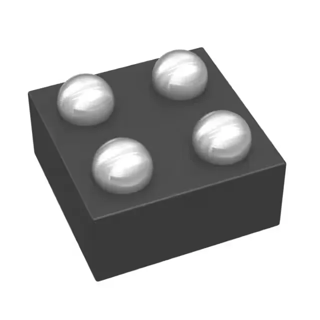
Package and board integration — 4-DSBGA (0.88x0.88)
The TPS22912CYZVT comes in a 4-bump DSBGA measuring 0.88 mm × 0.88 mm — the smallest footprint for a 2 A load switch in this family. The 0.5 mm pitch requires a solder-mask-defined pad with a stencil aperture matched to the bump diameter; a 0.25 mm aperture with 0.125 mm solder-mask clearance is typical for a 0.3 mm bump.
60 mOhm Rds(on) — conduction loss at 2 A
With a typical on-resistance of 60 mOhm, the TPS22912CYZVT dissipates 240 mW at 2 A continuous output. That 240 mW must be sunk through the four DSBGA bumps into the PCB — a 2-layer board with 1 oz copper and a 0.5-inch-square copper pour under the package keeps the junction rise under 40°C at 25°C ambient.
Slew-rate controlled — inrush management
The slew-rate controlled turn-on limits the inrush current into a capacitive load, preventing the upstream rail from drooping below the UVLO threshold of the switch itself or of other loads sharing the same supply. For a 10 µF load capacitor, the typical turn-on time is around 120 µs, keeping the inrush peak below 500 mA — well within the 2 A continuous rating. This matters in battery-powered designs where a sudden load step can trigger a brown-out reset on the MCU.