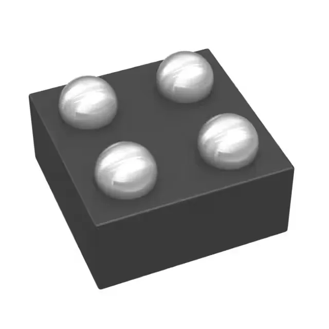
Package and board-fit for the 4-DSBGA
The TPS22902YFPR: This is a 4-bump wafer-level chip-scale package with no leads — the solder balls are the only interface to the board. The 0.5 mm pitch and 0.35 mm ball diameter demand a controlled solder-paste stencil and a fine-pitch placement head. The board-side pad finish should be OSP or ENIG to maintain coplanarity across the four bumps.
Output current and on-resistance — sizing the load
Rated for a continuous output current of 500 mA maximum, the TPS22902YFPR suits point-of-load switching for peripheral rails, sensor supplies, or low-power processor domains within the 1 V to 3.6 V load voltage range.
Switching behaviour and control interface
The switch is controlled by a single On/Off logic input (non-inverting) — a high level turns the P-channel FET on. No external Vcc/Vdd supply is required for the control logic; the gate drive is derived from the input voltage. Integrated slew-rate control limits inrush current during turn-on, reducing voltage droop on the input rail. The load discharge feature pulls the output to ground when the switch is off, preventing floating output nodes that could cause erratic behaviour in downstream logic.
Temperature grade and operating environment
The 4-DSBGA package has no exposed thermal pad — heat is conducted through the solder balls and board copper.