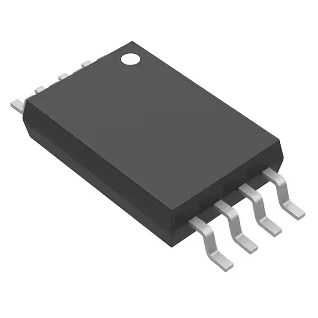
Power path selection for dual-supply designs
The Texas Instruments TPS2115APWRG4 is a source selector switch that routes one of two input power rails to a single output, with an internal N-Channel FET handling the switching. It is specified for handheld and mobile devices where a battery and a USB or adapter supply share the same load bus.
Current and voltage envelope for the BOM
Rated for a continuous output current of 1.25 A maximum, the TPS2115APWRG4 fits loads such as a sensor node radio, a small microcontroller, or a peripheral bus that draws under that ceiling. Quiescent supply current is 55 µA typical — low enough that the switch does not dominate the standby budget in a battery-powered product.
Switching timing and temperature grade
Turn-on delay is 1 ms and turn-off delay is 5 ms. These numbers matter for sequencing: the output rail ramps after the 1 ms delay, so the downstream load must tolerate that startup latency. The 5 ms off delay means the switch holds the output for 5 ms after the selected input drops — enough to ride through a brief supply glitch without toggling the load.