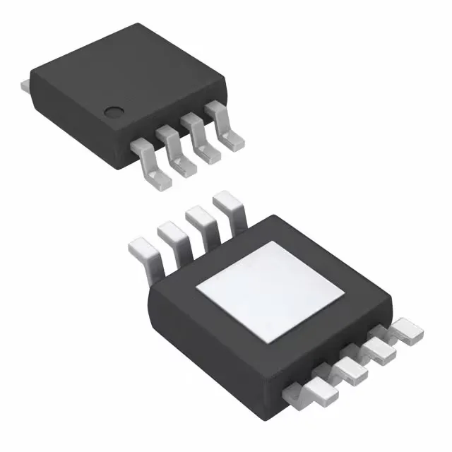
Texas Instruments TPS2065CDGNR — Analog & Data Acquisition

TI TPS2065CDGNR USB Power Switch, 1A, 86mOhm, 8-HVSSOP

MPNTPS2065CDGNR
End of Life

Texas Instruments TPS2065CDGNR USB power switch, 1A max output, 86mOhm typical Rds(on), high-side N-channel, 4.5V-5.5V load, 8-HVSSOP package, -40°C to 125°C.

$0.99Ref. price · indicative, final on quote
Packaging8-TSSOP, 8-MSOP (0.118", 3.00mm Width) Exposed Pad
StockContact for availability
MOQ1 pcs
  • 100% new & originalTraceable channels only — no refurbs, no pulls, no remarked parts.
  • Date & lot codes on quoteStated per line before you commit; label photos on request.
  • MSL-compliant ESD packingMoisture-sealed bags with indicator cards; reels photo-verified.
  • PayPal buyer protectionPay by T/T, PayPal or Payoneer — card payments covered end to end.

Specifications

TPS2065CDGNR Technical Specifications
ParameterValue
Input typeNon-Inverting
Output typeN-Channel
Switch typeUSB Switch
Mounting typeSurface Mount
Voltage - load4.5V ~ 5.5V
Voltage - supply (Vcc (Vdd))Not Required
Current - output1A
Number of outputs1
InterfaceOn/Off
Operating temperature-40°C ~ 125°C (TJ)
PackageTape & Reel (TR); Cut Tape (CT)
FeaturesLoad Discharge, Status Flag
Rds on86mOhm
Case8-TSSOP, 8-MSOP (0.118\", 3.00mm Width) Exposed Pad
Fault protectionCurrent Limiting (Fixed), Over Temperature, Reverse Current, UVLO
Output configurationHigh Side
Ratio - Input:Output1:1

Product details

USB power switch for downstream port protection

The Texas Instruments TPS2065CDGNR is a single-channel, high-side N-channel USB power switch rated for 1A continuous output with a typical on-resistance of 86mOhm. It integrates fixed current limiting, over-temperature protection, reverse-current blocking, and undervoltage lockout (UVLO) — the full set of fault protections needed for a robust USB downstream port. The switch is controlled by a single On/Off input (non-inverting) and provides a status flag output for fault reporting. The load-discharge feature ensures the output capacitor is bled when the switch is turned off, preventing residual voltage on the VBUS line.

86 mOhm Rds(on) — what it means for the BOM

At 1A load, the 86mOhm typical on-resistance produces roughly 86 mV drop. The industrial temperature range (-40°C to 125°C junction) means the switch can be used in outdoor telecom cabinets, factory-floor USB hubs, or engine-adjacent infotainment modules without derating concerns. The 8-HVSSOP package with exposed pad requires a thermal via pattern under the pad for the 1A continuous rating; the datasheet layout recommendation should be followed for full power dissipation.

Active production — no LTB risk

The TPS2065CDGNR carries an Active lifecycle status with ROHS3 compliance. For BOM stability, this part is a safe selection for new designs and ongoing production.

Frequently asked questions

What is the output current limit of TPS2065CDGNR?

The maximum continuous output current is 1A, with fixed current limiting as part of the fault protection set. The typical on-resistance is 86mOhm at that current.

Can TPS2065CDGNR be used in 3.3V systems?

The load voltage range is 4.5V to 5.5V, so this switch is designed for 5V USB VBUS rails, not 3.3V systems. For 3.3V power switching, a different device with a lower Vcc range would be needed.

TPS2065CDGNR thermal pad layout and power dissipation?

The 8-HVSSOP package has an exposed pad that must be soldered to a PCB thermal land with vias to a ground plane for effective heat dissipation. The datasheet provides the recommended land pattern and thermal via array. At 1A output with 86mOhm Rds(on), junction temperature rise is manageable within the -40°C to 125°C range, but the pad layout directly affects derating.