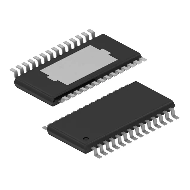
The THS7002IPWP: Surface-mount only. That PowerPAD underside needs a soldered thermal land on the PCB; without it the junction-to-board thermal path is broken and the part runs hotter than the datasheet's theta-JA assumes. Plan the copper pour on layer 2 as a solid ground island tied to the exposed pad.
What the 100 MHz bandwidth and 85 V/µs slew rate mean on the bench
The -3 dB bandwidth of 100 MHz and gain-bandwidth product of 70 MHz tell you this PGA can close a gain of 10 out to about 7 MHz before the open-loop roll-off eats the margin. A 10 kΩ source sees a 25 mV offset from bias alone before the 1 mV Vos is added. Keep the source impedance below 1 kΩ or account for the DC error in the downstream ADC range.
The THS7002IPWP operates from a single or split supply spanning 9 V to 32 V total. That 9 V minimum means it won't run from a 5 V rail — you need at least ±4.5 V or a single 9 V supply. The 32 V maximum covers ±15 V rails with headroom, which is the classic analog supply for high-swing signal chains. The 5 mA supply current per channel (10 mA total for both amplifiers) is modest for a 100 MHz part; the thermal dissipation in the HTSSOP package at 85°C ambient with both channels driving full output into 100 Ω is about 0.5 W, which the PowerPAD can handle with a reasonable copper area.