High-speed differential signal chain
The THS4503IDGN is a single-channel differential op-amp from Texas Instruments, designed for high-speed signal conditioning where a balanced output is needed — driving ADCs, transmitting over twisted-pair, or rejecting common-mode noise in a sensor front-end. With a 2800 V/µs slew rate and 370 MHz -3 dB bandwidth, this part handles fast edge rates in video distribution, radar IF processing, or communication receiver chains without slew-induced distortion. The gain-bandwidth product of 300 MHz means the closed-loop bandwidth scales inversely with gain — at a gain of 10, expect roughly 30 MHz of usable bandwidth before the open-loop roll-off dominates.
Supply and output drive
Operates from a single or split supply spanning 4.5 V to 15 V total — a ±5 V rail pair is a common configuration, giving enough headroom for a 2 Vpp differential output swing into a 100 Ω load. Each output channel can source or sink 120 mA, which is enough to drive a 50 Ω back-terminated cable or a moderate-capacitance ADC input buffer without an external line driver. Quiescent current is 23 mA per amplifier — modest for this speed class, but the thermal budget in the 8-HVSSOP package with exposed pad should be checked against the ambient temperature and output load.
Thermal and package considerations
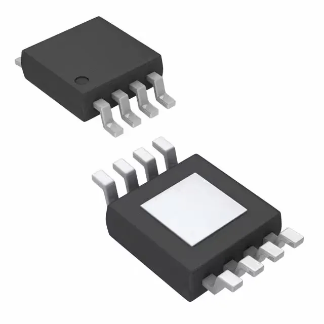
The 8-HVSSOP package (3.00 mm × 3.00 mm body with exposed thermal pad) requires a soldered copper land on the PCB to pull heat from the die — the datasheet's RθJA figure assumes a minimum of 2-layer board with thermal vias under the pad. Rated for -40°C to +85°C ambient operation, the part suits industrial control cabinets, base-station transceivers, and outdoor test equipment that sees temperature swings. Supplied in Tube format — the MSL (moisture sensitivity level) is not listed here, but the exposed pad construction typically carries MSL-3, meaning a bake before reflow if the shelf-life seal is broken.
Sourcing and compliance
ROHS3 compliant and lead-free — the termination finish is matte tin, compatible with standard lead-free reflow profiles (260°C peak).