Active production — no lifecycle risk on this BOM line
The THS4501IDGN: ROHS3 compliant per the manufacturer's declaration, so it passes the EU material restriction check without an exemption carve-out.
2800V/µs slew rate — what drives the fit
The 2800V/µs slew rate is the headline parameter here — it means this amplifier can swing its output at nearly 3 V per nanosecond. For a differential ADC driver driving a 2 Vpp signal into a high-speed SAR or pipeline converter, the settling time is dominated by the slew limit, not the small-signal bandwidth. If your signal chain needs to settle to 12-bit accuracy inside a 10 ns window, this part has the raw edge rate to do it. Paired with a 370 MHz -3dB bandwidth and 300 MHz gain-bandwidth product, the THS4501IDGN is sized for IF sampling, communications receive chains, and wideband instrumentation front-ends where the signal bandwidth exceeds 100 MHz.
Differential architecture and supply flexibility
True differential amplifier with differential output — this is not a single-ended op-amp configured as a difference amplifier. The input stage is balanced, and the output delivers a differential signal with common-mode rejection inherent to the topology. For driving the analog inputs of a differential ADC, this eliminates the need for an external transformer or a separate common-mode buffer. Supply span runs from 4.5 V to 15 V single or split supply. On a single 5 V rail the output swing is limited by the headroom, but on ±5 V or ±7.5 V the full 120 mA output current per channel is available. The 23 mA quiescent supply current is moderate for this speed class — expect about 115 mW dissipation on a ±5 V supply, which the exposed pad of the 8-HVSSOP handles with a modest copper pour. Industrial temperature range -40°C to 85°C covers most base-station, test-equipment, and industrial sensor environments. The 4 mV input offset voltage and 4 µA input bias current are typical for a high-speed bipolar process — the offset trims out in a DC-coupled path, and the bias current matters when the source impedance exceeds a few hundred ohms.
Package and PCB integration
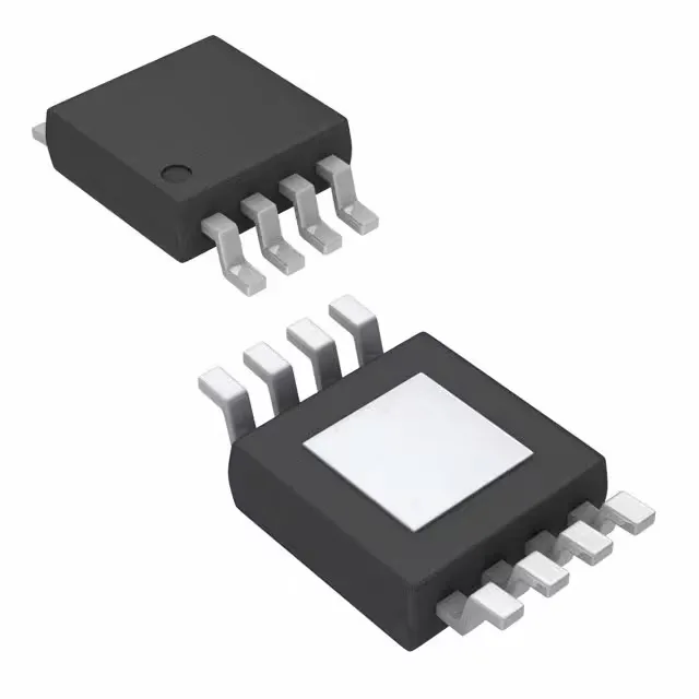
8-HVSSOP with exposed pad — the 3.00 mm × 3.00 mm body is small enough for dense channel cards, but the thermal pad underneath must be soldered to a ground-plane copper island with at least four thermal vias to keep the junction temperature below 125°C at full output swing. The tube packaging means the parts ship in anti-static tubes of 80 or 100, not tape-and-reel — factor that into your pick-and-place feeder setup if you are running high-volume reels. Surface-mount only — no through-hole variant exists. The 0.65 mm pin pitch on the MSOP footprint is standard; the exposed pad is the centre tab connected to V– on this device. Confirm your layout connects the pad to the negative supply or leaves it floating per the datasheet recommendation — it is not a thermal-only pad.