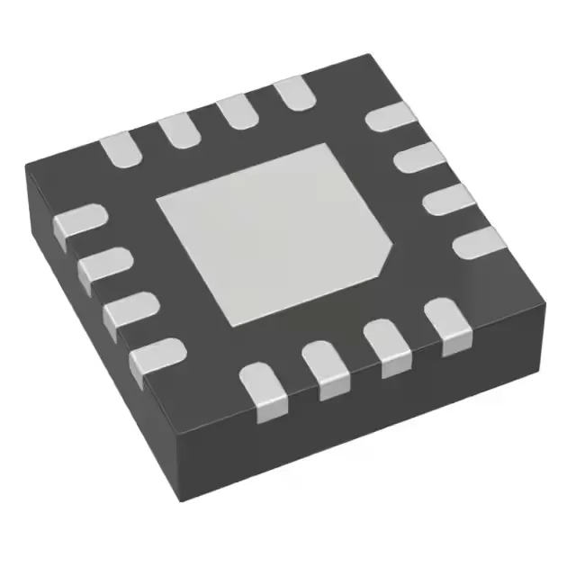
Its 2.4 GHz -3 dB bandwidth and 5500 V/µs slew rate put it squarely in the territory of RF/IF amplifier stages, high-speed ADC drivers, and pulse-processing front-ends where settling time and large-signal response matter. The part runs from a 3 V to 5 V supply span and draws 37 mA quiescent current — a deliberate trade-off: you get the speed, but you budget the rail current accordingly. The 16-VQFN (3x3) package with exposed pad keeps the thermal path short; the pad needs a solid via array to the ground plane if you plan to push the output swing near the rails at high frequency.
The 5500 V/µs slew rate supports output swings of several volts in under a nanosecond.
The 16-VQFN (3x3) with exposed pad is a compact, low-inductance package — good for high-frequency performance, but it demands a rework station with a hot-air nozzle that matches the 3 mm body. Pin 1 is marked by a dot on the top of the package; the pad pattern is symmetric, so double-check orientation before placing. A stencil with a single large aperture for the pad, rather than an array of small ones, gives better solder coverage and void control.