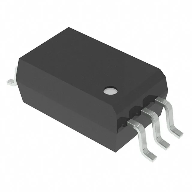
Automotive-grade isolated gate driver with 4.5A peak drive
The UCC23313BQDWYRQ1 is a single-channel isolated gate driver built on capacitive coupling technology, delivering 4.5 A peak source and 5.3 A peak sink current — enough to drive the gate charge of medium-power IGBTs and SiC MOSFETs in automotive traction inverters or DC-DC converters without an external booster stage. Rated for 3750 Vrms isolation, it meets the reinforced isolation requirements for motor-drive and on-board charger applications where galvanic separation between the control and power stages is mandatory. The 150 kV/µs common-mode transient immunity ensures the output stays clean when the power stage switches at high dv/dt — a common failure point in fast-switching SiC designs where the ground bounce can corrupt the gate signal.
AEC-Q100 qualification and automotive deployment
UL and VDE approval on the isolation barrier means the part carries the safety certifications required for automotive-grade power modules and traction systems sold into regulated markets.
Supply range and timing margins for gate-drive design
The output supply range of 10 V to 33 V covers the typical gate-drive voltages for IGBTs (15 V) and SiC MOSFETs (18-20 V) from a single rail, with headroom for the bootstrap diode drop in half-bridge topologies. Propagation delay is 105 ns max matched between rising and falling edges, with pulse-width distortion held to 35 ns — tight enough to keep the dead-time budget in a 20-50 kHz switching inverter without overcompensating in firmware. Rise and fall times of 28 ns and 25 ns respectively mean the gate driver can charge and discharge the input capacitance of a 30 nC IGBT in under 150 ns, limiting the switching losses in the Miller plateau region.
6-SOIC package and board integration
Housed in a 6-pin SOIC wide-body (7.50 mm width), the package provides 8 mm creepage distance between input and output sides — sufficient for 600 V working voltage systems with reinforced isolation per IEC 60747-17.