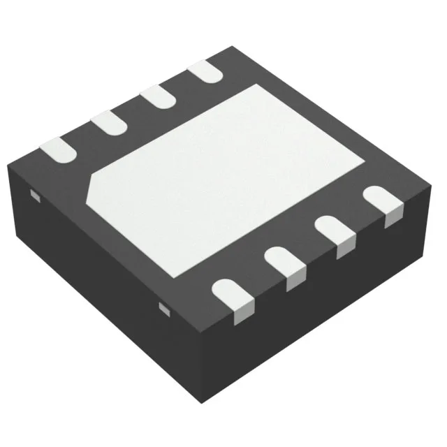
Slew rate and bandwidth — what they mean for signal fidelity
The THS4215DRBT delivers a 970 V/µs slew rate with a 325 MHz -3 dB bandwidth and a 350 MHz gain-bandwidth product. For a voltage-feedback amplifier, the slew rate sets the large-signal full-power bandwidth — the maximum output voltage swing at a given frequency before distortion rises. A 970 V/µs rate supports a 10 V peak-to-peak swing up to roughly 15 MHz, making this part suited for pulse amplifiers, video distribution, or ADC drivers where the output must slew through the full rail without slew-rate limiting. The 350 MHz gain-bandwidth product means the closed-loop -3 dB bandwidth equals 350 MHz divided by the noise gain. At a gain of +10, expect 35 MHz small-signal bandwidth — enough for a 10 MSPS ADC front-end or a high-speed data acquisition channel.
Operating from a single supply between 5 V and 15 V, the THS4215DRBT fits into 5 V or 12 V systems without a negative rail. The 19 mA quiescent supply current is moderate for this speed class — in a multi-channel array of four amplifiers, the total supply draw stays under 80 mA, which a standard linear regulator can source without a heatsink. The 3 mV typical input offset voltage and 7 µA input bias current set the DC accuracy floor. For a transimpedance amplifier with a 10 kΩ feedback resistor, the 7 µA bias produces a 70 mV DC error term — this matters when the signal is a photodiode current in the microamp range. The 7 µA bias is higher than a FET-input amplifier, so the source impedance should be kept below a few kilo-ohms to avoid excessive DC offset.
Package and board integration
Without this, the junction temperature rises above the 85°C maximum under continuous high-slew-rate operation. Surface-mount assembly with tape-and-reel packaging supports automated pick-and-place for production volumes. The cut-tape option is available for prototype or low-volume builds.
ROHS3 compliant, with no exemptions for lead in solder or other restricted substances. No AEC-Q automotive qualification is listed, so this part is not screened for under-hood or chassis-mounted applications.