What the 7300 V/µs slew rate means on the bench
The THS3091DDA is a single-channel current-feedback op amp with a 7300 V/µs slew rate — that is the large-signal edge rate, not the small-signal bandwidth. For a 10 V output step, the rise time is about 1.4 ns; the output slews at that rate until the signal amplitude drops below the slew-limiting threshold, after which the 235 MHz -3 dB bandwidth governs the small-signal response. Rated output current is 280 mA per channel, which means it can drive low-impedance loads like a 50 Ω transmission line directly without a separate buffer stage. The current-feedback architecture keeps the slew rate nearly independent of the closed-loop gain — useful when you need the same edge rate across different gain settings.
Package and thermal: the PowerPad matters
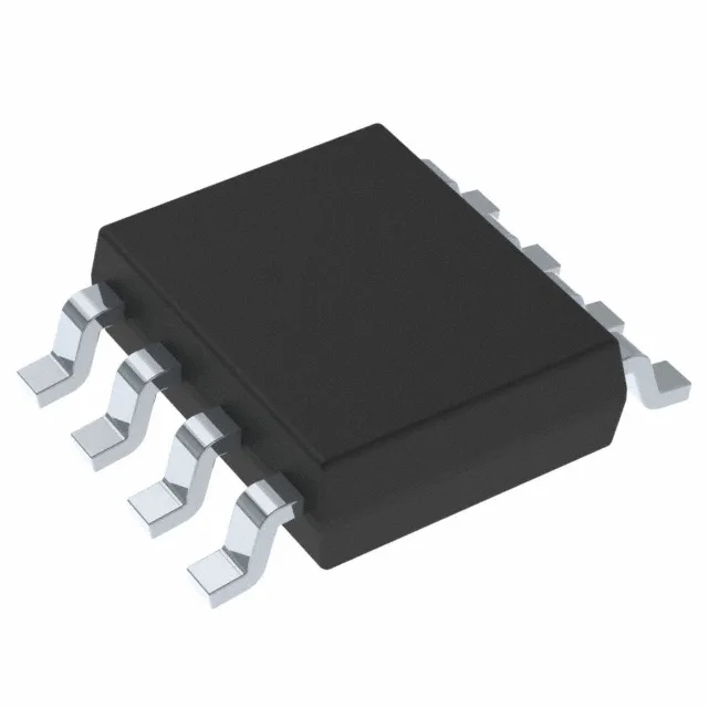
Housed in an 8-PowerSOIC (0.154", 3.90 mm width) with the exposed thermal pad on the bottom — the 8-SO PowerPad supplier package variant. The pad must be soldered to a copper plane on the PCB to pull heat out of the die; without it, the 9.5 mA supply current plus the output stage dissipation will push the junction temperature past the 85 °C ambient ceiling in still air. Surface-mount only, shipped in a tube. The 4 µA input bias current and 900 µV input offset voltage are typical for a current-feedback design running at these speeds — expect to trim the offset if the signal chain requires DC accuracy below a few millivolts.
Supply rails and temperature range
Operates from a 10 V to 30 V total supply span — that is the difference between the positive and negative rails, not a single-ended supply. A ±5 V to ±15 V split supply fits within that range. The -40 °C to 85 °C operating temperature covers industrial environments; no automotive qualification (AEC-Q) is listed.