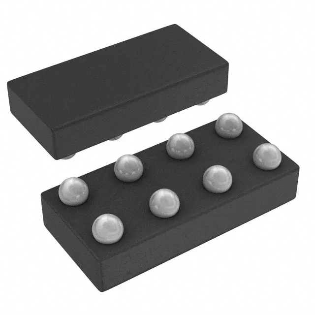
Dual 2-input AND gate in a 0.5 mm-pitch BGA
The SN74LVC2G08YZTR is a dual 2-input AND gate from the 74LVC series, packing two independent AND functions into an 8-bump DSBGA package (0.5 mm pitch). Each gate can source or sink 32 mA at the output, enough to drive a standard CMOS input or a low-power LED indicator without a buffer. The 3.8 ns propagation delay at 5 V, 50 pF load keeps the gate fast enough for most control and data-path logic below 100 MHz. Quiescent current maxes at 10 µA across the full supply range, so it adds negligible draw in battery-powered or always-on subsystems.
Package and board-fit realities for the DSBGA
The 8-DSBGA package (8 bumps, 0.5 mm pitch) requires a PCB with fine-line traces and a solder-mask-defined pad. The 0.5 mm pitch means a 4-layer board is typical for fan-out; two-layer designs may struggle to route all signals without vias under the package. Stencil aperture for the DSBGA should match the bump diameter (approx 0.3 mm) with a 1:1 ratio; a 100 µm thick stencil is standard. The package is moisture-sensitive — bake before reflow if the floor life has been exceeded.