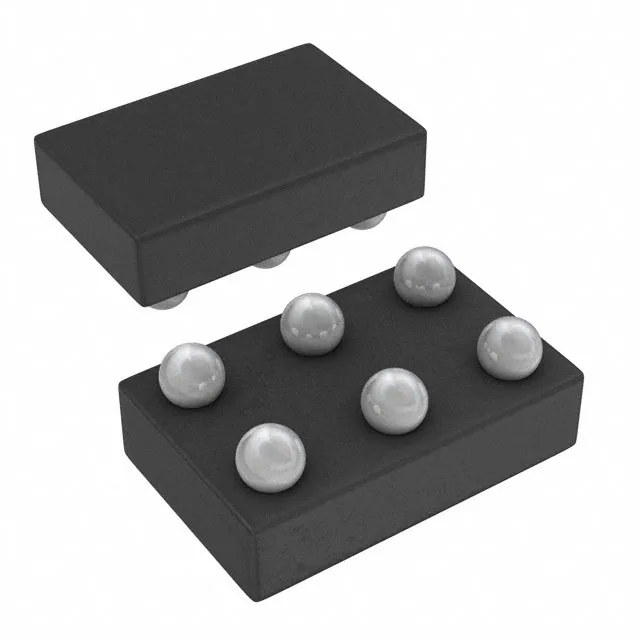
Dual inverter with open-drain outputs — 2.9 ns propagation delay at 5 V
The SN74LVC2G06YZPR: Each channel provides an open-drain output, meaning the output can sink current but cannot source it — the pull-up resistor is external, allowing the output voltage to be set independently of the supply rail, useful for level translation or wired-OR bus structures. The 2.9 ns maximum propagation delay at 5 V with a 50 pF load sets the data-rate ceiling — at 3.3 V the delay is slightly higher, but still well under 5 ns for most SPI or GPIO interfaces.
The open-drain output sinks up to 32 mA per channel, sufficient to drive a low-power LED, a relay coil with a flyback diode, or a logic input with a weak pull-up. The high-level output current is listed as "—" because the output does not source current — the pull-up resistor handles the sourcing, and the 32 mA figure is the maximum the NMOS can pull low without exceeding the package thermal limit. Quiescent current is 10 µA maximum, so the part adds negligible standby draw in battery-powered designs. Input logic thresholds are specified: low-level 0.7 V to 0.8 V, high-level 1.7 V to 2 V, consistent with the 1.65 V minimum supply.
Active production — ROHS3 compliant, no obsolescence concern
The 6-DSBGA package (0.5 mm pitch, 0.9 mm x 1.4 mm body) requires careful PCB layout — the solder mask opening and stencil aperture must match the TI recommended land pattern to avoid solder bridging.