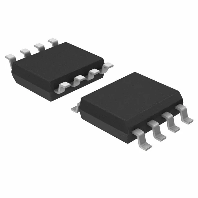
Dual NAND in a tight spot
The SN74LVC2G00DCT3 is a dual 2-input NAND gate from TI's 74LVC family, packing two independent gates into an 8-pin SM8 package (8-LSSOP / 8-MSOP, 2.80 mm wide).
What the 3.8 ns propagation delay means on the bench
Max propagation delay is 3.8 ns at 5 V driving a 50 pF load — that is the timing budget for the signal to settle before the next clock edge. At 1.65 V the delay stretches, so for a 50 MHz bus the 3.3 V supply rail is the safer bet. Quiescent current maxes at 10 µA across the whole supply range — the part barely sips power when the inputs are static, which matters for battery-powered sensor nodes that spend most of their time asleep.
Package and swap-ability in the field
SM8 is a small-outline package with a 0.65 mm pitch — doable with a fine-tip iron and some flux if you are swapping it on a bench, but the 2.80 mm body width means the pads are close together. A hot-air station at 300°C with a small nozzle is cleaner for removal. The part is surface-mount only — no through-hole equivalent in this family.