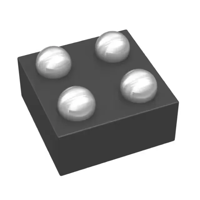
Texas Instruments SN74LVC1G34YZVR — Interface & Transceivers

SN74LVC1G34YZVR Single-Gate Buffer, 1.65V-5.5V, DSBGA-4

MPNSN74LVC1G34YZVR
Active

Texas Instruments 74LVC series SN74LVC1G34YZVR, Buffer, Non-Inverting, 1.65V ~ 5.5V supply, 32mA output, -40°C ~ 85°C, 4-DSBGA (0.88x0.88mm) package.

$0.1577Ref. price · indicative, final on quote
Independent supplier — new & surplus stockAuthenticity-screened · ESD-safe packingListing updated Aug 2026

Specifications

SN74LVC1G34YZVR specifications
ParameterValue
Series74LVC
Logic typeBuffer, Non-Inverting
Output typePush-Pull
MountingSurface Mount
Supply voltage1.65V ~ 5.5V
Current - output high, low32mA, 32mA
Operating temperature-40°C~85°C(TA)
PackageTape & Reel (TR); Cut Tape (CT)
Case4-XFBGA, DSBGA
Number of elements1
Number of bits per element1

Product details

Single-gate buffer in a sub-1mm BGA — what you're working with

It's a bare-die-scale BGA, not a molded leadframe package — the bumps are on the bottom, no leads to inspect, and the footprint is essentially the silicon outline plus a tiny fanout.

It's compatible with 3.3 V logic without any extra translation — the input thresholds scale with VCC. The 32 mA symmetric output drive (source and sink) is generous for a single-gate part; you can drive a low-current LED, a few CMOS inputs, or a short stub of trace without needing a separate driver.

The DSBGA package's thermal performance is adequate at these temperatures as long as the PCB has a reasonable copper plane under the bump array.

Package reality — DSBGA assembly notes

The 4-DSBGA (0.88 x 0.88 mm) is a wafer-level chip-scale package. MSL is not stated in this listing, but typical TI DSBGA parts are MSL 1 or 2; verify the reel label before bake decisions. The tiny footprint means the PCB pad design must follow the TI application note for DSBGA land patterns — a continuous copper pad under the package with via-in-pad if routing out requires it. Tombstoning risk is negligible because the bumps are symmetric and the part is light, but stencil aperture and solder paste volume matter for consistent joint formation.

For BOM planning, there is no forced obsolescence risk on the horizon.

Frequently asked questions

Is SN74LVC1G34YZVR compatible with 3.3V logic?

Yes. Input and output levels scale with VCC, making it fully compatible with 3.3 V CMOS and TTL logic without external translation.

What is the direct equivalent for SN74LVC1G34YZVR in a different package?

The base product number is 74LVC1G34, and TI offers this same buffer function in several packages: the SN74LVC1G34DBVR (SOT-23-5) and SN74LVC1G34DCKR (SC-70-5) are common leaded alternatives. The electrical specs (supply range, drive current, temperature grade) are identical across the package variants — only the footprint and assembly process differ.