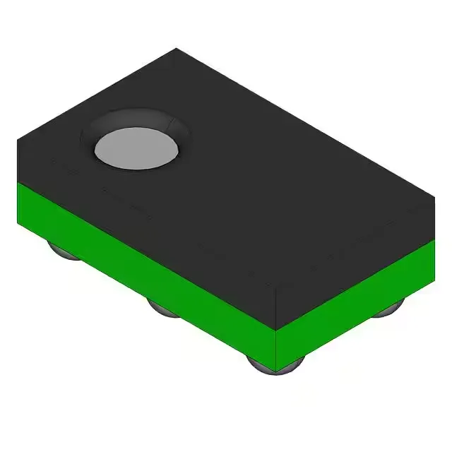
Texas Instruments SN74LVC1G34YZTR — Interface & Transceivers

SN74LVC1G34YZTR Buffer, Non-Inverting, 1.65V-5.5V, 32mA

MPNSN74LVC1G34YZTR
End of Life

Texas Instruments 74LVC series single-gate buffer, non-inverting, push-pull output, 1.65V to 5.5V supply, 32mA output drive, 5-DSBGA package, -40°C to 85°C operating temperature.

Sourced new & surplus through independent channelsAuthenticity-screened · ESD-safe packingListing updated Aug 2026

Specifications

SN74LVC1G34YZTR specifications
ParameterValue
Series74LVC
Logic typeBuffer, Non-Inverting
Output typePush-Pull
MountingSurface Mount
Voltage1.65V ~ 5.5V
Current - output high, low32mA, 32mA
Operating temperature-40°C~85°C(TA)
PackageTape & Reel (TR)
Case5-UFBGA, DSBGA
Number of elements1
Number of bits per element1

Product details

Single-gate buffer for mixed-voltage signal conditioning

The Texas Instruments SN74LVC1G34YZTR is a single-gate non-inverting buffer from the 74LVC logic family, in a 5-bump DSBGA package. The push-pull output delivers 32mA source and sink, enough to drive a modest LED, a logic input fan-out of several loads, or a short PCB trace.

The wide supply range is the headline feature. A 1.8V microcontroller talking to a 3.3V peripheral? This buffer sits between them, powered from the 3.3V rail, and the input thresholds track the supply so a 1.8V logic-high is recognised as a valid high. The same part works in a 5V legacy bus without a separate level shifter. One line item on the BOM covers multiple voltage interfaces, which simplifies procurement and qualification.

32mA output drive — enough for real loads

The 32mA push-pull output is not just for logic fan-out. It can directly drive a small indicator LED with a series resistor, or buffer a clock signal across a short backplane trace. The symmetrical source and sink current means the output waveform stays balanced, reducing duty-cycle distortion on a 1 MHz clock line. For heavier loads, the same family offers 50mA variants, but for most board-level buffering 32mA is the sweet spot.

No last-time-buy notice, no end-of-life schedule. This part is qualified for ongoing production and new designs. The 5-DSBGA package is a standard TI offering, so supply continuity is solid. For dual-sourcing, the same die is available in SOT-23 and SC-70 packages (SN74LVC1G34DBVR, SN74LVC1G34DCKR) if the board can accommodate a larger footprint.

Frequently asked questions

What is the difference between SN74LVC1G34 and SN74LVC1G125?

Both are single-gate buffers from the 74LVC family, but the SN74LVC1G125 adds a 3-state output enable pin. The SN74LVC1G34 is a simple non-inverting buffer with no enable — the output always follows the input. If you need bus isolation or shared-line control, choose the SN74LVC1G125. For a fixed buffer path, the SN74LVC1G34 is the simpler, lower-cost choice.

Can SN74LVC1G34 be used as a level shifter?

Yes. The SN74LVC1G34 can translate between voltage domains because its input thresholds scale with VCC. For example, power the device at 3.3V, and a 1.8V logic-high is recognised as a valid high. The output swings rail-to-rail at 3.3V. This works for unidirectional level shifting up to the supply voltage. For bidirectional translation, a dedicated level shifter like the TXB0104 is needed.