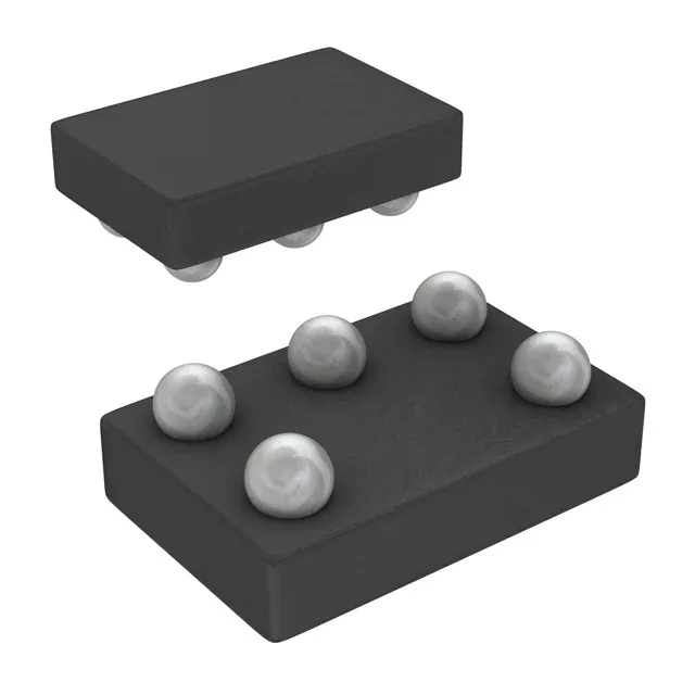
Single-gate buffer in a DSBGA — what the 1.4x0.9 footprint means for placement
The SN74LVC1G34YZPR is a single-element, non-inverting buffer from TI's 74LVC logic family. The push-pull output delivers 32mA source and sink, which is unusually high for a single-gate buffer — enough to drive a modest LED, a relay coil through a resistor, or a long PCB trace without an external line driver. That 1.4x0.9 footprint is the whole story for board layout: it needs a solder-paste stencil designed for 0.3 mm pitch bumps, and rework requires hot-air with underfill removal.
32 mA output drive — why it matters for your load budget
Most single-gate 74LVC buffers spec 24 mA typical; this part's 32 mA gives extra headroom for driving capacitive loads on long clock or reset lines, or for interfacing to optocouplers and small relays. The supply range from 1.65V to 5.5V means it can sit on a 3.3V rail and still accept 5V inputs without damage, or run at 1.8V for a low-voltage FPGA I/O bank.
Active lifecycle — no last-time-buy clock ticking
TI lists the SN74LVC1G34YZPR as Active — current production, no end-of-life notice. The base product number 74LVC1G34 covers a family of pin-compatible packages (SOT-23, SC-70, SOT-553), so if the DSBGA footprint becomes a supply bottleneck, the same die in a leaded package is a drop-in alternative with a different PCB land pattern.