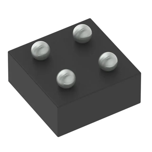
Single-gate buffer for mixed-voltage and space-constrained boards
The SN74LVC1G34DPWR: It operates from a 1.65V to 5.5V supply, bridging legacy 5V logic with modern 1.8V or 3.3V cores without a level translator. The push-pull output delivers 32mA source and sink, enough to drive a handful of CMOS loads or a short PCB trace cleanly. Housed in a 4-X2SON package measuring 0.8x0.8mm, it fits into tight sensor modules, portable devices, and I/O expansion headers where every square millimeter counts.
The 1.65V to 5.5V supply range means this single gate can sit on a 1.8V FPGA bank, a 3.3V MCU rail, or a 5V legacy peripheral bus without a separate regulator. That flexibility simplifies the power tree and reduces BOM line count. If you need to drive a longer run or a heavier capacitive load, budget a series resistor to keep the edge rate under control.
The 125°C ceiling means it survives near an engine bay or a hot power supply without derating the output drive. No AEC-Q100 qualification is listed, so for production automotive safety-critical paths, verify the grade against your program requirements.
Package reality — the 4-X2SON footprint
The 4-X2SON (0.8x0.8mm) package is a tiny leadless SON with an exposed pad. Hand-soldering this package is impractical — plan for machine placement and reflow.
For production BOM lines, this part presents no LTB risk and is straightforward to dual-source with other 74LVC1G34 variants in different packages if needed.