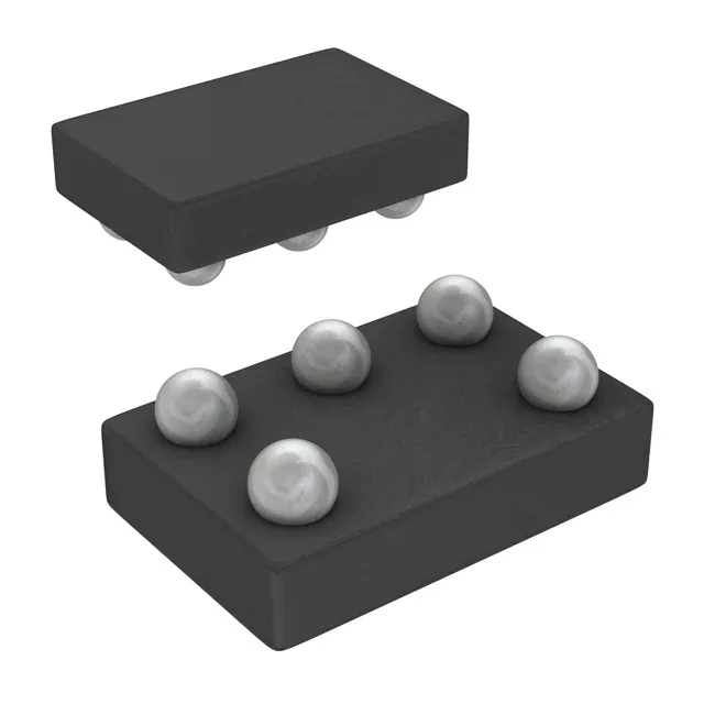
It operates from a 1.65V to 5.5V supply and can source or sink 32mA per channel, making it suitable for driving LEDs, relay coils, or logic inputs across mixed-voltage boards. The 5-DSBGA package (1.4x0.9 mm) is a wafer-level chip-scale package — no leads, no exposed pad — designed for space-constrained assemblies where a standard SOT-23 or SC-70 footprint won't fit.
If the board can tolerate a package change, the more common SN74LVC1G126DCK (SOT-23-5) or SN74LVC1G126DBV (SOT-23-5) are still active and widely stocked, but they are not pin-compatible with the DSBGA land pattern.
The wide supply range lets this buffer bridge a 1.8V MCU to a 3.3V or 5V peripheral without a separate level shifter. The 32mA symmetric drive at both logic highs and lows is enough to switch a small signal relay or a MOSFET gate through a series resistor. The 3-state output allows multiple buffers to share a bus line — useful in multiplexed address or data lines where the output goes high-impedance when not selected.
5-DSBGA — assembly and rework considerations
It requires a PCB land pattern with 0.5 mm pitch and a solder-mask-defined pad. Rework is difficult — the package is fragile and typically requires hot-air rework with a preheat plate. For prototyping or low-volume production, the SOT-23-5 variant (SN74LVC1G126DCK) is easier to hand-solder and probe, though the footprint is different.