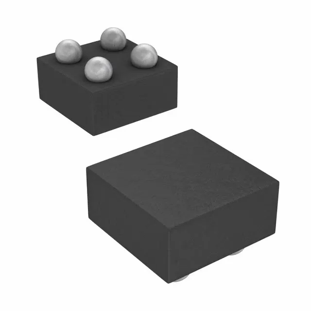
Texas Instruments SN74LVC1G06YZTR — Interface & Transceivers

SN74LVC1G06YZTR – TI 74LVC Single Buffer/Driver, Open Drain

MPNSN74LVC1G06YZTR
End of Life

Texas Instruments 74LVC series, Buffer, Inverting, 1 Element, 1 Bit per Element, Open Drain Output, 4-UFBGA/DSBGA, Surface Mount, 1.65V~5.5V Supply, -40°C~85°C.

Sourced new & surplus through independent channelsAuthenticity-screened · ESD-safe packingListing updated Aug 2026

Specifications

SN74LVC1G06YZTR specifications
ParameterValue
Series74LVC
Logic typeBuffer, Inverting
Output typeOpen Drain
MountingSurface Mount
Voltage1.65V ~ 5.5V
Current - output high, low-, 32mA
Operating temperature-40°C~85°C
PackageTape & Reel (TR)
Case4-UFBGA, DSBGA
Number of elements1
Number of bits per element1

Product details

Single-gate open-drain buffer in a 0.9 mm DSBGA

The SN74LVC1G06YZTR: The open-drain output sinks 32 mA. The 4-DSBGA package measures 0.9 mm × 0.9 mm.

The open-drain output is the key feature here. Unlike a push-pull output, the open-drain stage can only pull the output low (sink current); the high level is determined by an external pull-up resistor to whatever voltage rail you choose. It also enables wired-OR connections where multiple open-drain outputs share a common pull-up, useful for interrupt lines or I²C-like buses. The 32 mA sink capability is generous for a single-gate device, so driving an indicator LED directly is fine, but check the total package dissipation if you run near that limit continuously.

DSBGA package — tiny footprint, careful rework

The balls are small and the package has no leads to grab with an iron — rework requires hot air and a stencil or preform for the solder paste. The 0.9 mm pitch means the PCB footprint needs tight registration; a solder mask defined pad is recommended. Pin 1 identification on a 4-ball DSBGA is usually a corner ball marked by a dot or a chamfer on the package edge; verify the orientation mark before placement.

The base product number 74LVC1G06 covers multiple package variants, so if the DSBGA version becomes constrained, a pin-compatible alternative in a larger package (e.g., SOT-23 or SC-70) may be available — but verify the footprint compatibility; the DSBGA is unique.

Frequently asked questions

Can SN74LVC1G06YZTR be used at 3.3V?

Yes. The supply voltage range is 1.65 V to 5.5 V, so 3.3 V is well within the operating window. The open-drain output can be pulled up to any voltage within the absolute maximum ratings, typically up to 5.5 V.

What is the difference between SN74LVC1G06YZTR and SN74LVC1G06DRLR?

The two parts share the same logic function (single inverting buffer with open-drain output) and electrical specifications. The difference is the package: the YZTR suffix is the 4-DSBGA (0.9 mm × 0.9 mm), while the DRLR suffix is a SOT-553 package (1.6 mm × 1.6 mm). The DSBGA is smaller but harder to rework by hand; the SOT-553 is larger and more assembly-friendly. The pinout is not the same, so they are not drop-in replacements on the same PCB footprint.