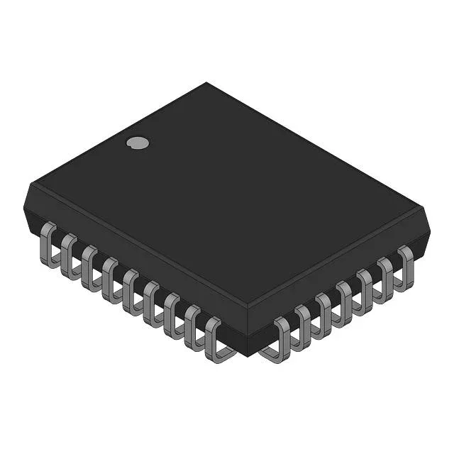
Active production, no last-time-buy clock ticking
Texas Instruments lists the SN74ACT7201LA35RJ as Active.
35 ns access, 512 x 9 — what that means on the bench
The 35 ns access time sets the read-cycle floor: the data appears on the outputs within 35 ns of the read-enable edge. For a 22.22 MHz asynchronous data rate, that gives roughly 45 ns per cycle — the access time fits with margin for the downstream latch setup. The 4.5 Kbit memory is organised 512 words deep by 9 bits wide. Nine bits means eight data plus one parity or control bit per word — common in telecom and datacom buffers where a ninth bit carries out-of-band signalling. Retransmit capability lets the FIFO re-present the same data on a subsequent read cycle without the source resending it — handy for error-retry sequences or diagnostic loops where the host wants to re-examine a buffer segment.
32-PLCC — field-swappable with a standard tool
The 32-PLCC (J-Lead) package is a surface-mount part with the leads bent under the body. It can be removed and replaced with a standard soldering iron and wick — no hot-air station or reflow oven required. That matters when you are swapping a FIFO on a customer site or in a repair depot without a full SMT lab. Package / Case is 32-LCC (J-Lead) — the JEDEC PLCC footprint. The J-lead gives a visual solder-joint inspection under magnification, unlike a QFN or BGA where the joints are hidden.
Supply and temperature — standard 5 V logic lane
The 80 mA max supply current means the part stays cool without a heatsink even at full toggle rate; a standard 100 mA LDO or 5 V rail tap handles it. Fine for office, lab, telecom central office, or indoor industrial control cabinets. Not rated for -40°C automotive or outdoor enclosures without climate control.
Asynchronous — no clock tree, no PLL
Asynchronous operation means the FIFO uses separate read and write strobes with no common clock. The 22.22 MHz data rate is the maximum frequency at which the control signals can toggle — no clock skew budget to manage, no PLL lock time. The trade-off is that the designer must respect the 35 ns access time on the read side and the write-pulse width on the write side. No FWFT (First-Word Fall-Through) support and no programmable flags — the flag outputs (Empty, Full, Half-Full) are hard-wired logic, not configurable. Simpler control interface, fewer register writes to configure, but less flexibility for custom watermarks.
Depth and width expansion — cascading for larger buffers
Expansion type is Depth and Width — multiple SN74ACT7201LA35RJ devices can be cascaded to create deeper or wider FIFO arrays. Depth expansion chains the Empty/Full flags; width expansion connects the control lines in parallel and fans out the data bus. The PLCC footprint makes board layout straightforward for a multi-chip array. Bus direction is Uni-Directional — data flows one way through the FIFO. For bidirectional buffering you need two devices back-to-back or a different part. The 9-bit width means a single device handles an 8-bit data bus plus parity, or a 9-bit serial protocol word.