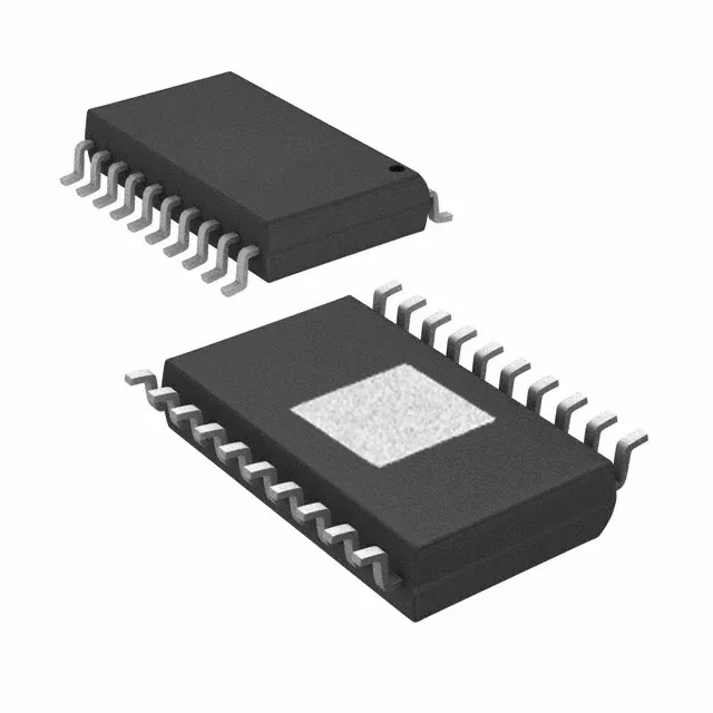
2.4 A output op-amp for high-drive loads
The OPA569AIDWP is a single-channel, general-purpose operational amplifier from Texas Instruments that delivers 2.4 A of output current per channel — enough to directly drive a motor winding, a solenoid, or a high-power LED string without an external buffer stage. With a gain-bandwidth product of 1.2 MHz and a slew rate of 1.2 V/µs, it is sized for moderate-speed control loops and signal conditioning where the load current dominates the design choice, not the bandwidth.
Rail-to-rail output and wide supply range
The rail-to-rail output stage swings within millivolts of the supply rails, preserving headroom when the load pulls the output near the supply limit — important in a 2.4 A driver where every volt of drop is dissipated as heat in the die. Supply span runs from 2.7 V to 5.5 V, covering single-cell Li-ion through regulated 5 V rails, so the same BOM line serves portable and line-powered designs. Quiescent supply current is 9 mA — the part does not idle hot even when the output is not sourcing load current, which matters in a thermally constrained 20-HSOIC package.
20-HSOIC exposed-pad thermal management
The 20-SOIC package with exposed pad (0.295-inch body width, 7.50 mm) routes the die's heat through the pad to the PCB copper plane — the layout must include a thermal land and vias to a ground plane to keep the junction temperature within the -40°C to 85°C operating range under continuous 2.4 A load. Surface-mount assembly on the 20-HSOIC footprint; the exposed pad is the primary thermal path, so the solder paste coverage under the pad should match the recommended stencil aperture in the TI application note.
DC precision for the signal chain
Input offset voltage is 500 µV maximum, and input bias current is 1 pA typical at 25°C — the bias current doubles every 10°C, so at 85°C it sits around 64 pA, still negligible for a 10 kΩ source but a factor in a high-impedance sensor front-end. These DC specs mean the OPA569AIDWP can serve as the drive stage in a precision current source or as the output buffer in a DAC signal chain without adding an appreciable error term.
Active production and compliance
The part is ROHS3 Compliant, meeting the latest EU restriction directive without exemption.