150 MHz GBW and 80 V/µs slew rate — signal-chain bandwidth anchor
The OPA2301AIDGKT: The 150 MHz gain-bandwidth product sets the closed-loop bandwidth ceiling for a given noise gain — at a gain of 10, the -3 dB point lands at 15 MHz, which covers video, high-speed ADC drivers, and wideband instrumentation front-ends. 0.1 pA typical input bias current eliminates the need for a guard ring or bootstrapping on a high-impedance sensor front-end — a 10 MΩ source resistor drops only 1 µV of offset from bias current, negligible in a 1 mV offset amplifier.
Dual-channel CMOS with 9.5 mA per channel supply
Two independent CMOS amplifiers in a single 8-VSSOP package, each drawing 9.5 mA quiescent current — total 19 mA for the dual, which fits a 5 V rail budget of 95 mW quiescent dissipation. 70 mA output current per channel drives the input of a 12-bit, 10 MSPS SAR ADC directly, or a 50 Ω back-terminated cable with 3.5 V swing — the output stage is not limited to high-impedance loads. The 2.7 V minimum allows the amplifier to run from a lithium-ion cell near end-of-discharge.
The operating temperature range covers the full industrial envelope and the under-hood automotive ambient — an engine control unit (ECU) or transmission controller that sees 105°C on the PCB still has 20°C margin before the top of the range. 1 mV maximum input offset voltage over temperature means the DC accuracy is consistent across the range — a thermocouple amplifier with a gain of 100 sees only 100 mV of output-referred offset drift, manageable with a software calibration routine.
8-VSSOP — footprint and layout notes
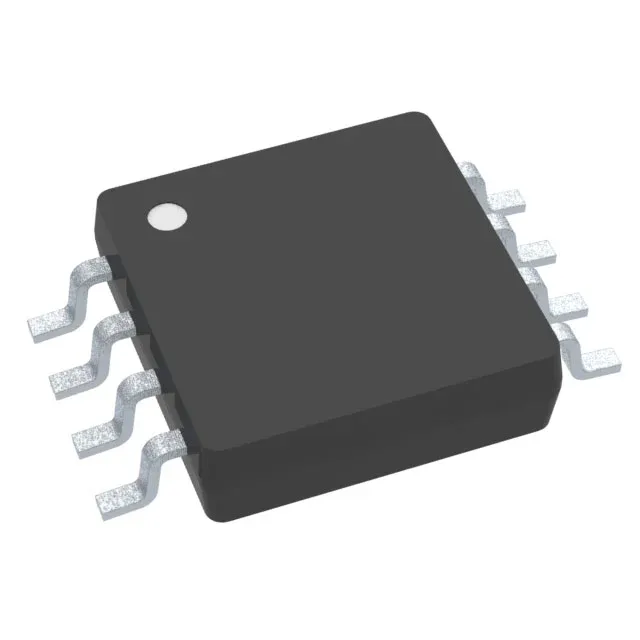
The 8-VSSOP package (3.00 mm × 3.00 mm body, 0.65 mm pitch) fits on a two-layer board with a 0.20 mm trace width — the centre pad is not a thermal pad, so no via array under the package is needed; place a 0.1 µF decoupling capacitor within 2 mm of each supply pin. Cut Tape works for prototype builds and rework.
Active lifecycle and compliance
ROHS3 compliant — no exemption-flagged substances; the package is lead-free and compatible with lead-free reflow profiles (260°C peak).