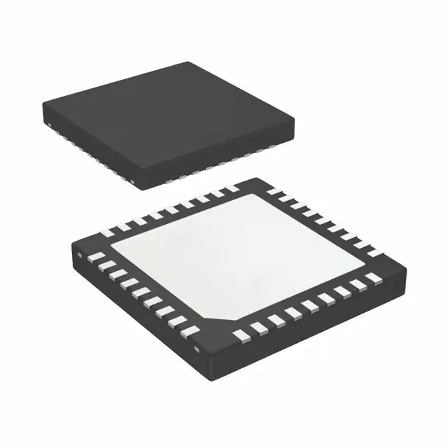
What this RF synthesizer does for your clock tree
The LMX2541SQ3030E/NOPB is a PLL-based frequency synthesizer with an integrated VCO, designed to generate clean clock signals up to 3.23 GHz from a reference clock input. It's a single-chip solution for RF synthesis in wireless infrastructure, test equipment, or any design needing a stable, programmable carrier.
Why the 3.23 GHz ceiling matters for your RF budget
The 3.23 GHz maximum output frequency sets the upper bound for the carrier or LO you can synthesize directly. If your design needs a 2.4 GHz ISM-band or a 3.5 GHz WiMAX carrier, this part covers it with margin. The integrated VCO saves you from designing a separate oscillator and loop filter — the PLL and VCO are on the same die, which simplifies layout and reduces board area. The 2:2 input-to-output ratio means you can distribute two independent clock outputs from a single reference, useful for feeding multiple mixer or ADC clock inputs from one synthesizer.
The 36-WQFN (6x6 mm) package with exposed pad is hand-solderable with a hot-air station — the pad underneath needs a thermal via pattern for proper heat sinking.
What about a second-source like CD74HCT7046AE?
The CD74HCT7046AE is a through-hole PLL from the 74HCT logic family, running at 38 MHz max with a 4.5V supply. It is not a functional replacement for the LMX2541SQ3030E/NOPB — the frequency range, supply voltage, and package are completely different. No direct second-source exists for this RF synthesizer; the LMX2541SQ3030E/NOPB is a unique TI part.