130 kHz gain bandwidth for precision low-frequency signal chains
The LMP2232BMMX/NOPB is a dual general-purpose op-amp from the LMP® series, built for applications where supply current is tight and offset drift matters. Its 130 kHz gain-bandwidth product sets the usable closed-loop bandwidth; for a gain of 100, the signal path stays flat to roughly 1.3 kHz, making it a fit for thermocouple conditioning, strain-gauge amplification, and battery-monitoring front-ends that run below 1 kHz. Each of the two channels draws 19 µA total supply current, placing this part in the micropower class. At that quiescent level, the op-amp can remain powered continuously in a sensor node that wakes every few seconds to sample and transmit, without draining the primary cell.
10 µV offset and 0.02 pA bias — direct sensor interface without trimming
Together they allow the op-amp to connect directly to high-impedance sources such as pH probes, pyroelectric detectors, or photodiodes without an external nulling circuit. The bias current is so low that a 10 MΩ source resistor contributes only 0.2 µV of additional offset — negligible in a 10 µV system. A 3.3 V rail yields a 3.3 V output swing into a 10 kΩ load, enough headroom for a 12-bit ADC reference.
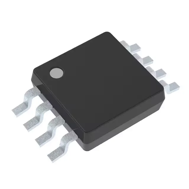
Housed in an 8-VSSOP — the 3.00 mm × 3.00 mm footprint with 0.65 mm pitch fits on a two-layer board without micro-vias. The operating temperature range spans -40°C to 125°C, covering under-hood automotive, industrial enclosure, and outdoor telecom cabinet environments. Slew rate is 0.058 V/µs; with the 130 kHz GBW, the part slews cleanly on a 1 V step in about 17 µs, adequate for DC and low-frequency AC signals.