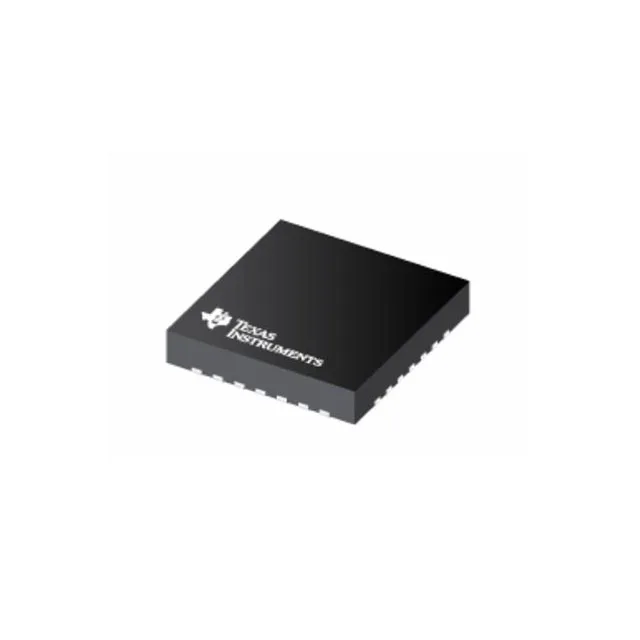
2 GHz fanout buffer with multi-protocol input flexibility
Each of the two independent fanout circuits distributes one input to four matched outputs, making it a compact building block for high-speed clock trees in networking, telecom, and data-center equipment where signal integrity and low additive jitter matter.
That makes it a straightforward choice for production BOMs where long-term availability is a requirement. For dual-sourcing or a pin-compatible alternative, the CDCLVP1204RGTR is a functional peer but uses LVPECL outputs and a single 1:2 fanout topology — the output logic family and fanout ratio differ, so a straight swap requires board-level changes.
Package and footprint notes for layout
The wettable-flank terminals aid optical inspection and solder-joint reliability. Supply decoupling should follow the recommended layout in the datasheet — one 0.1 µF cap per supply pin pair, placed as close as possible to the VQFN edge.