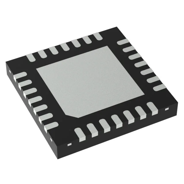
The Texas Instruments LMK1D1204PRHDT is a 2:4 differential clock buffer designed to distribute high-speed reference clocks with minimal additive jitter. It accepts one differential input and delivers four differential outputs, each capable of running up to 2 GHz. That frequency ceiling puts it squarely in the range needed for 10+ Gbps SERDES reference clocks, PCIe Gen 4/5, 100GbE, and CPRI/OBSAI base station links. The part accepts any of three supply rails — 1.8V, 2.5V, or 3.3V — so it can drop into an existing power domain without a dedicated LDO. The 28-VQFN (5x5 mm) package keeps the footprint small enough for dense line cards.
Supply voltage flexibility — one buffer, three rails
The LMK1D1204PRHDT operates from any of three supply ranges: 1.71V to 1.89V, 2.375V to 2.625V, or 3.135V to 3.465V. That means it runs on a nominal 1.8V, 2.5V, or 3.3V rail without level shifters. For a design that already has a clean 1.8V supply for the FPGA bank, this buffer can share that rail. If the board uses 2.5V for the clock synthesizer, the same part works. The wide tolerance on each range — ±5% on 1.8V, ±5% on 2.5V, ±4.8% on 3.3V — covers the typical regulator output tolerance plus some IR drop.
Differential I/O — signal integrity at multi-GHz speeds
Both the input and the four outputs are differential, supporting LVDS, LVPECL, HCSL, and CML signal levels. Differential signaling rejects common-mode noise and maintains clean edge rates at 2 GHz, which is essential when the clock trace runs across a backplane or through a connector. The 2:4 ratio means one PLL or oscillator output can feed four receiver loads — typically FPGA reference clock banks, SerDes transceivers, or Ethernet PHYs — without degrading the signal integrity that a multi-drop single-ended topology would suffer.
That includes outdoor telecom cabinets, base stations, industrial Ethernet switches, and test equipment that sits in unconditioned factory floors. The 28-VQFN with exposed pad helps pull heat into the PCB ground plane when the part is running near its temperature limit.
The active status means no last-time-buy risk for new designs.