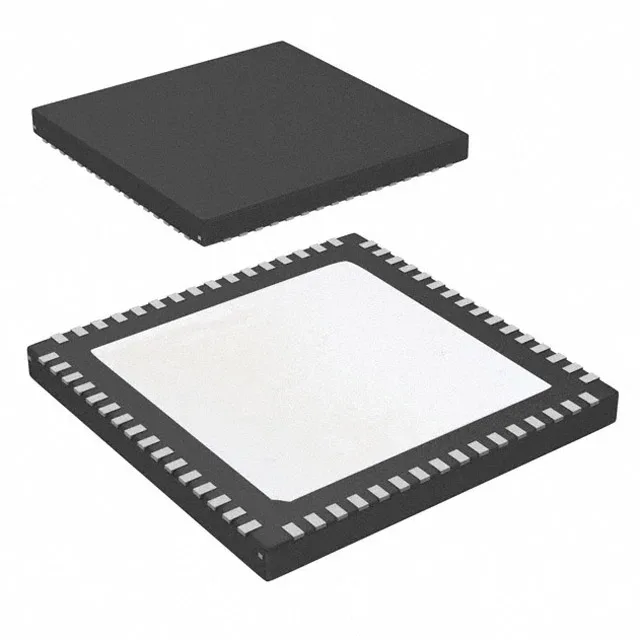
The LMK04906BISQX/NOPB is a PLLatinum clock generator from Texas Instruments built around a phase-locked loop core with an integrated VCO that hits 2.6 GHz maximum output frequency. It accepts LVCMOS, LVDS, or LVPECL on the input side and delivers the same three logic families on the output — no level-shifting resistors between the reference oscillator and the downstream dividers. The 3:6 input-to-output ratio means three selectable clock sources feed six device outputs, enough to clock a multi-card chassis or a data converter array without external fan-out buffers. All six outputs are differential-capable, so the pair count covers three LVDS or LVPECL clock trees.
The supply range is 3.15 V to 3.45 V — a tight 3.3 V ±4.5 % window that demands a clean regulator; this is not a wide-VIN part for noisy backplane rails. The pad also serves as the low-inductance ground return for the PLL core — skipping the vias risks both thermal shutdown and phase-noise degradation.
That means no last-time-buy scramble for ongoing builds, and the part qualifies for new designs without a sunset risk.
What the 2.6 GHz ceiling buys you
The 2.6 GHz maximum output frequency covers the LO generation range for most cellular bands through mid-band 5G, satellite downconverters, and test equipment local oscillators. Below that ceiling, the PLL's divider chain can synthesise any sub-harmonic frequency the reference allows — the jitter-cleaning bandwidth is set by the loop filter components, not the VCO range. Because the part accepts and outputs LVCMOS, LVDS, and LVPECL, a single BOM line can drive a mixed-signal board where the ADC demands LVDS clocking, the FPGA uses LVPECL, and a control monitor runs LVCMOS — all from the same PLL device.