Jitter cleaning with PLLatinum architecture
The LMK04828BISQX/NOPB is a PLL-based jitter cleaner from TI's PLLatinum series, designed to reduce phase noise on clock signals in high-speed data converter and RF sampling applications. With a maximum output frequency of 3.08 GHz, it supports clocking for gigasample ADCs, FPGA transceivers, and SerDes interfaces where timing margin is the bottleneck. The 3:15 input-to-output ratio lets a single reference clock fan out to fifteen devices, reducing the number of discrete clock buffers and simplifying the clock tree.
Multi-protocol I/O and signal integrity
Inputs accept LVCMOS, LVDS, and LVPECL levels, while outputs can be configured as HSDS, LCPECL, LVCMOS, LVDS, or LVPECL — covering the common high-speed logic families without external level translation. Differential input and output paths are supported, which preserves signal integrity over longer board traces and reduces common-mode noise coupling into the clock distribution. The single PLL circuit (Number of Circuits: 1) is paired with an integrated VCO and loop filter, minimizing external component count and layout sensitivity.
Industrial temperature range and package integration
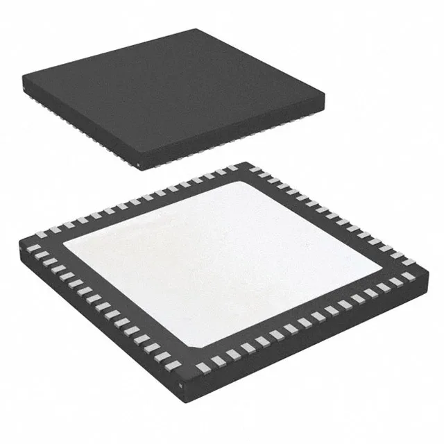
Housed in a 64-WFQFN with exposed pad (9x9 mm), the package requires a thermal via array under the pad to sink heat from the PLL and output drivers into the PCB ground plane. Supply voltage range is 3.15 V to 3.45 V — a clean 3.3 V rail with adequate decoupling at the package pins is needed to keep PLL in-band noise below the datasheet floor.
The base product number LMK04828 identifies the family; the suffix BISQX/NOPB indicates the specific temperature grade, package, and tape-and-reel packaging option.