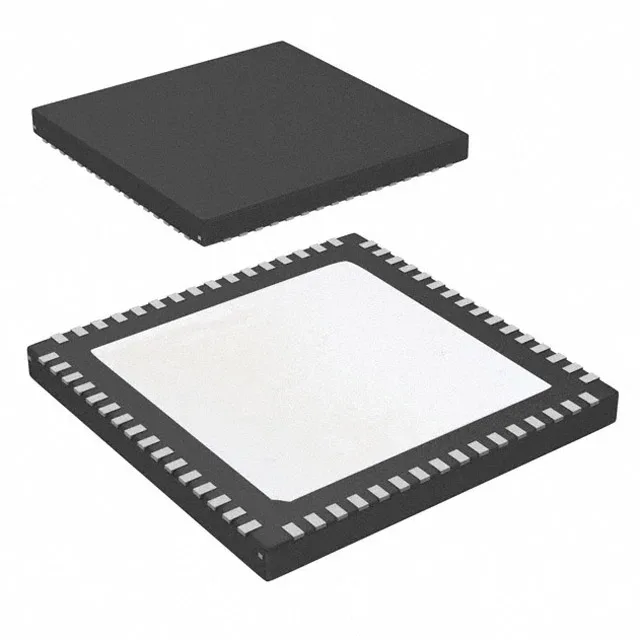
2.5 GHz jitter cleaner — the PLL core and what it drives
The LMK04826BISQE/NOPB: This is a PLL-based jitter cleaner from the PLLatinum™ series, with a maximum output frequency of 2.5 GHz. The integrated PLL locks to a reference and attenuates phase noise on the clock — the jitter-cleaning bandwidth is set by the loop filter, which you size for the application's phase-noise profile. The 3:15 input-to-output ratio means three reference inputs feed fifteen differential or single-ended clock outputs — enough to clock an entire ADC/DAC card or a multi-channel data-acquisition backplane without external fan-out buffers. All input and output pairs accept or deliver LVCMOS, LVDS, and LVPECL levels, plus HSDS and LCPECL on the output side. That covers the common clocking standards in wireless infrastructure, radar, and high-speed test equipment.
Supply rail and temperature — the operating envelope
The device requires a 3.15 V to 3.45 V supply. The PLL's VCO and charge pump are sensitive to supply ripple — the datasheet's recommended decoupling scheme (page 7 of the full datasheet) places 0.1 µF and 1 µF caps at each supply pin, with the exposed paddle soldered to a quiet ground plane for thermal and electrical reference. The 64-WQFN (9x9 mm) exposed-pad package requires a thermal via array under the paddle to keep the junction temperature within limits when the device is clocking multiple outputs at 2.5 GHz.
Sourcing and supply posture
The base product number LMK04826 covers the family variants; confirm the package code (BISQ) and tape-and-reel suffix (/NOPB) match your assembly line's feeder setup.